SLLSEE5D february 2013 – july 2023 TUSB8040A1
PRODUCTION DATA
- 1
- 1Features
- 2Applications
- 3Description
- 4Revision History
- 5Pin Configuration and Functions
- 6Specifications
-
7Detailed Description
- 7.1 Overview
- 7.2 Functional Block Diagram
- 7.3 Memory
- 7.4 I2C EEPROM Operation
- 7.5 SMBus Target Operation
- 7.6
Configuration Registers
- 7.6.1 ROM Signature Register
- 7.6.2 Vendor ID LSB Register
- 7.6.3 Vendor ID MSB Register
- 7.6.4 Product ID LSB Register
- 7.6.5 Product ID MSB Register
- 7.6.6 Device Configuration Register
- 7.6.7 Battery Charging Support Register
- 7.6.8 Device Removable Configuration Register
- 7.6.9 Port Used Configuration Register
- 7.6.10 Reserved Register
- 7.6.11 Reserved Register
- 7.6.12 Language ID LSB Register
- 7.6.13 Language ID MSB Register
- 7.6.14 Serial Number String Length Register
- 7.6.15 Manufacturer String Length Register
- 7.6.16 Product String Length Register
- 7.6.17 Reserved Register
- 7.6.18 Serial Number Registers
- 7.6.19 Manufacturer String Registers
- 7.6.20 Product String Registers
- 7.6.21 Additional Feature Configuration Register
- 7.6.22 Reserved Register
- 7.6.23 Reserved Register
- 7.6.24 Device Status and Command Register
-
8Applications, Implementation, and Layout
- 8.1 Application Information
- 8.2
Typical Application
- 8.2.1 Design Requirements
- 8.2.2
Detailed Design Procedure
- 8.2.2.1 Upstream Port Implementation
- 8.2.2.2 Downstream Port 1 Implementation
- 8.2.2.3 Downstream Port 2 Implementation
- 8.2.2.4 Downstream Port 3 Implementation
- 8.2.2.5 Downstream Port 4 Implementation
- 8.2.2.6 VBUS Power Switch Implementation
- 8.2.2.7 Clock, Reset, I2C/SMBUS, and Misc
- 8.2.2.8 Power Implementation
- 8.2.3 Application Curve
- 8.2.4 Power Supply Recommendations
- 8.2.5
Layout
- 8.2.5.1
Layout Guidelines
- 8.2.5.1.1 Part Placement
- 8.2.5.1.2
Board Layout Considerations
- 8.2.5.1.2.1 RKM Package – QFN (Quad Flat No-Lead)
- 8.2.5.1.2.2 Impedance
- 8.2.5.1.2.3 Critical Signals
- 8.2.5.1.2.4 Crystal
- 8.2.5.1.2.5 USB Interface
- 8.2.5.1.2.6 Differential Pair Signals
- 8.2.5.1.2.7 Port Connectors
- 8.2.5.1.2.8 Reset Terminals
- 8.2.5.1.2.9 Miscellaneous Terminals
- 8.2.5.1.2.10 Power Control and Battery Charging Terminals
- 8.2.5.1.2.11 USB 2.0 Port Indicator LED Terminals
- 8.2.5.1.3 Power
- 8.2.5.2 Layout Example
- 8.2.5.1
Layout Guidelines
- 9Device and Documentation Support
- Mechanical, Packaging, and Orderable Information
Package Options
Mechanical Data (Package|Pins)
- RKM|100
Thermal pad, mechanical data (Package|Pins)
- RKM|100
Orderable Information
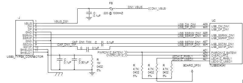
8.2.2.4 Downstream Port 3 Implementation
 Figure 8-5 Downstream Port 3 Implementation
The downstream port 3 of the TUSB8040A1 is connected to a USB3 Type A connector. With PWRON2z_BATEN2 pin pulled-up, battery charge support is enabled for the port. If battery charge support is not needed, the internal pull-down resistor will disable it by default. Also, the internal pull-up resistors on the LEDG2z_USED2 and LEDA2z_RMBL2 pins mark the port as functional and device removable (for the opposite, external pull-downs are required).