SLDS250A December 2019 – May 2022 TUSS4440
PRODUCTION DATA
- 1 Features
- 2 Applications
- 3 Description
- 4 Revision History
- 5 Pin Configuration and Functions
-
6 Specifications
- 6.1 Absolute Maximum Ratings
- 6.2 ESD Ratings
- 6.3 Recommended Operating Conditions
- 6.4 Thermal Information
- 6.5 Power-Up Characteristics
- 6.6 Transducer Drive
- 6.7 Receiver Characteristics
- 6.8 Echo Interrupt Comparator Characteristics
- 6.9 Digital I/O Characteristics
- 6.10 Switching Characteristics
- 6.11 Typical Characteristics
- 7 Detailed Description
- 8 Application and Implementation
- 9 Power Supply Recommendations
- 10Layout
- 11Device and Documentation Support
- 12Mechanical, Packaging, and Orderable Information
Package Options
Mechanical Data (Package|Pins)
- RTJ|20
Thermal pad, mechanical data (Package|Pins)
- RTJ|20
Orderable Information
8.2.1 Transformer Drive Configuration Options
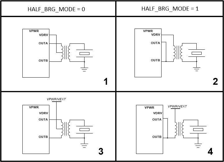
The TUSS4440 supports two pulsing modes to accommodate specific system needs based on the transformer used as shown in Figure 8-2. The typical application diagram in Figure 8-1 is considered as "Case 1".
 Figure 8-2 TUSS4440 Transducer Drive Options
The behavior of the internal FETs of TUSS4440 is different for each configuration in Table 8-2. The relationship between the IOx pins and the state of the OUTA and OUTB pins for different register settings is shown in Table 8-2 and Table 8-3.
Table 8-2 OUTA / OUTB Pin Behavior for Different Drive Configurations in IO MODE 2
| IO MODE 2 | ||||||
|---|---|---|---|---|---|---|
| START OF BURST | HALF_BRG_MODE | IO1 | IO2 | OUTA | OUTB | APPLICATION CASE |
| YES | 0 | 0 | 0 | Hi-Z | Hi-Z | CASE 1, CASE 3 |
| 0 | 0 | 1 | Hi-Z | GND | ||
| 0 | 1 | 0 | GND | Hi-Z | ||
| NO | 0 | 1 | 1 | Hi-Z | Hi-Z | |
| YES | 1 | 0 | 0 | Hi-Z | Hi-Z | CASE 2, CASE 4 |
| 1 | 0 | 1 | GND | GND | ||
| 1 | 1 | 0 | Hi-Z | Hi-Z | ||
| NO | 1 | 1 | 1 | Hi-Z | Hi-Z | |
Table 8-3 OUTA / OUTB Pin Behavior for Different Drive Configurations in IO MODE 0, IO MODE 1 and IO MODE 3
| IO MODE 0, IO MODE 1, IO MODE 3 | |||||||
|---|---|---|---|---|---|---|---|
| START OF BURST | HALF_BRG_MODE | CMD_TRIGGER (IO MODE 0) | IO1 (IO MODE 1) | IO2 | OUTA | OUTB | APPLICATION CASE |
| NO | 0 | 0 | 1 | 0 | Hi-Z | Hi-Z | CASE 1, CASE 3 |
| 0 | 0 | 1 | 1 | ||||
| YES | 0 | 1 | 0 | 0 | Hi-Z | GND | |
| 0 | 1 | 0 | 1 | GND | Hi-Z | ||
| NO | 1 | 0 | 1 | 0 | Hi-Z | Hi-Z | CASE 2, CASE 4 |
| 1 | 0 | 1 | 1 | ||||
| YES | 1 | 1 | 0 | 0 | Hi-Z | Hi-Z | |
| 1 | 1 | 0 | 1 | GND | GND | ||