SLVSEQ4A September   2018  – December 2018 TVS2201

PRODUCTION DATA.  

  1. Features
  2. Applications
  3. Description
    1.     Device Images
      1.      Voltage Clamp Response to 8/20-µs Surge Event
      2.      Functional Block Diagram
  4. Revision History
  5. Device Comparison Table
  6. Pin Configuration and Functions
    1.     Pin Functions
  7. Specifications
    1. 7.1 Absolute Maximum Ratings
    2. 7.2 ESD Ratings - JEDEC
    3. 7.3 ESD Ratings - IEC
    4. 7.4 Recommended Operating Conditions
    5. 7.5 Thermal Information
    6. 7.6 Electrical Characteristics
    7. 7.7 Typical Characteristics
  8. Detailed Description
    1. 8.1 Overview
    2. 8.2 Functional Block Diagram
    3. 8.3 Feature Description
    4. 8.4 Device Functional Modes
      1. 8.4.1 Protection Specifications
      2. 8.4.2 Reliability Testing
      3. 8.4.3 Zero Derating
      4. 8.4.4 Bidirectional Operation
      5. 8.4.5 Transient Performance
  9. Application and Implementation
    1. 9.1 Application Information
    2. 9.2 Typical Application
      1. 9.2.1 Design Requirements
      2. 9.2.2 Detailed Design Procedure
      3. 9.2.3 Application Curves
  10. 10Power Supply Recommendations
  11. 11Layout
    1. 11.1 Layout Guidelines
    2. 11.2 Layout Example
  12. 12Device and Documentation Support
    1. 12.1 Documentation Support
      1. 12.1.1 Related Documentation
    2. 12.2 Receiving Notification of Documentation Updates
    3. 12.3 Community Resources
    4. 12.4 Trademarks
    5. 12.5 Electrostatic Discharge Caution
    6. 12.6 Glossary
  13. 13Mechanical, Packaging, and Orderable Information

Package Options

Mechanical Data (Package|Pins)
Thermal pad, mechanical data (Package|Pins)
Orderable Information

Pin Configuration and Functions

DRB Package
8-Pin SON
Top View
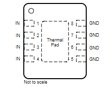
TVS2201 DRB Package.gif

Pin Functions

PIN TYPE DESCRIPTION
NAME DRB
IN 1, 2, 3, 4 IN Surge Protected Channel
GND 5, 6, 7, 8 GND Ground
FLOAT Exposed Thermal Pad NC Exposed Thermal Pad Must Be Floating