SCES640J january 2007 – july 2023 TXS0102
PRODUCTION DATA
- 1
- 1 Features
- 2 Applications
- 3 Description
- 4 Revision History
- 5 Pin Configuration and Functions
-
6 Specifications
- 6.1 Absolute Maximum Ratings
- 6.2 ESD Ratings
- 6.3 Recommended Operating Conditions
- 6.4 Thermal Information
- 6.5 Electrical Characteristics
- 6.6 Timing Requirements: VCCA = 1.8 V ±0.15 V
- 6.7 Timing Requirements: VCCA = 2.5 V ± 0.2 V
- 6.8 Timing Requirements: VCCA = 3.3 V ± 0.3 V
- 6.9 Switching Characteristics: VCCA = 1.8 V ± 0.15 V
- 6.10 Switching Characteristics: VCCA = 2.5 V ± 0.2 V
- 6.11 Switching Characteristics: VCCA = 3.3 V ± 0.3 V
- 6.12 Typical Characteristics
- 7 Parameter Measurement Information
- 8 Detailed Description
- 9 Application and Implementation
- 10Device and Documentation Support
- 11Mechanical, Packaging, and Orderable Information
Package Options
Mechanical Data (Package|Pins)
Thermal pad, mechanical data (Package|Pins)
- DQM|8
Orderable Information
7 Parameter Measurement Information
Unless otherwise noted, all input pulses are supplied by generators having the following characteristics:
- PRR 10 MHz
- ZO = 50 W
- dv/dt ≥ 1 V/ns
Note: All parameters and waveforms are
not applicable to all devices.
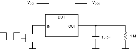
 Figure 7-1 Data Rate, Pulse Duration,
Propagation Delay, Output Rise
 And Fall Time Measurement Using A Push-Pull Driver
 Figure 7-2 Data Rate, Pulse Duration,
Propagation Delay, Output Rise
 And Fall Time Measurement Using An Open-Drain Driver
 Figure 7-3 Load Circuit For Enable /
Disable Time Measurement
Figure 7-3 Load Circuit For Enable /
Disable Time MeasurementTable 7-1 Switch Configuration For
Enable / Disable Timing
| TEST | S1 |
|---|---|
| tPZL(2), tPLZ (1) | 2 × VCCO |
| tPHZ(1), tPZH(2) | Open |
(1) tPLZ and tPHZ are the same as
tdis.
(2) tPZL and tPZH are the same as
ten.

(1) All input
pulses are measured one at a time, with one transition per measurement.
Figure 7-4 Voltage Waveforms Pulse
Duration
(1) All input pulses
are measured one at a time, with one transition per measurement.
Figure 7-5 Voltage Waveforms Propagation
Delay Times
(1) Waveform 1 is
for an output with internal conditions such that the output is low, except when
disabled by the output control.
(2) Waveform 2 is
for an output with internal conditions such that the ouput is high, except when
disabled by the output control.
Figure 7-6 Voltage Waveforms Enable And
Disable Times