SCES973A June 2024 – September 2024 TXS0102V-Q1
PRODUCTION DATA
- 1
- 1 Features
- 2 Applications
- 3 Description
- 4 Pin Configuration and Functions
-
5 Specifications
- 5.1 Absolute Maximum Ratings
- 5.2 ESD Ratings
- 5.3 Recommended Operating Conditions
- 5.4 Thermal Information
- 5.5 Electrical Characteristics
- 5.6 Switching Characteristics, VCCA = 1.8 ± 0.15 V
- 5.7 Switching Characteristics, VCCA = 2.5 ± 0.2 V
- 5.8 Switching Characteristics, VCCA = 3.3 ± 0.3 V
- 5.9 Switching Characteristics: Tsk, TMAX
- 5.10 Typical Characteristics
- 6 Parameter Measurement Information
- 7 Detailed Description
- 8 Application and Implementation
- 9 Device and Documentation Support
- 10Revision History
- 11Mechanical, Packaging, and Orderable Information
Package Options
Refer to the PDF data sheet for device specific package drawings
Mechanical Data (Package|Pins)
- DCU|8
Thermal pad, mechanical data (Package|Pins)
Orderable Information
3 Description
This two-bit non-inverting translator is a bidirectional voltage-level translator and can be used to establish digital switching compatibility between mixed-voltage systems. It uses two separate configurable power-supply rails, with the A ports supporting operating voltages from 1.65V to 3.6V while it tracks the VCCA supply, and the B ports supporting operating voltages from 2.3V to 5.5V while it tracks the VCCB supply. This allows the support of both lower and higher logic signal levels while providing bidirectional translation capabilities between any of the 1.8V, 2.5V, 3.3V, and 5V voltage nodes.
When the output-enable (OE) input is low, all I/Os are placed in the high-impedance state, which significantly reduces the power-supply quiescent current consumption.
To put the device in the high-impedance state during power up or power down, OE should be tied to GND through a pulldown resistor; the current-sourcing capability of the driver determines the minimum value of the resistor.
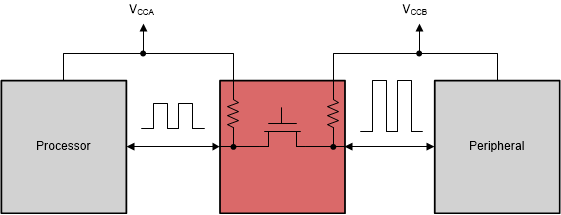
 Typical Application Block Diagram for TXS0102V-Q1