SCES973A June 2024 – September 2024 TXS0102V-Q1
PRODUCTION DATA
- 1
- 1 Features
- 2 Applications
- 3 Description
- 4 Pin Configuration and Functions
-
5 Specifications
- 5.1 Absolute Maximum Ratings
- 5.2 ESD Ratings
- 5.3 Recommended Operating Conditions
- 5.4 Thermal Information
- 5.5 Electrical Characteristics
- 5.6 Switching Characteristics, VCCA = 1.8 ± 0.15 V
- 5.7 Switching Characteristics, VCCA = 2.5 ± 0.2 V
- 5.8 Switching Characteristics, VCCA = 3.3 ± 0.3 V
- 5.9 Switching Characteristics: Tsk, TMAX
- 5.10 Typical Characteristics
- 6 Parameter Measurement Information
- 7 Detailed Description
- 8 Application and Implementation
- 9 Device and Documentation Support
- 10Revision History
- 11Mechanical, Packaging, and Orderable Information
Package Options
Refer to the PDF data sheet for device specific package drawings
Mechanical Data (Package|Pins)
- DCU|8
Thermal pad, mechanical data (Package|Pins)
Orderable Information
7.3.1 Architecture
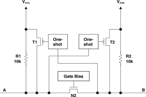
The TXS0102V-Q1 architecture (see Figure 7-1) is an auto-direction-sensing based translator that does not require a direction-control signal to control the direction of data flow from A to B or from B to A.
 Figure 7-1 Architecture of a TXS0102V-Q1 Cell
These two bidirectional channels independently determine the direction of data flow without a direction-control signal. Each I/O pin can be automatically reconfigured as either an input or an output, which is how this auto-direction feature is realized.
The TXS0102V-Q1 device is part of TI's "Switch" type voltage translator family and employs two key circuits to enable this voltage translation:
- An N-channel pass-gate transistor topology that ties the A-port to the B-port
- Output one-shot (O.S.) edge-rate accelerator circuitry to detect and accelerate rising edges on the A or B ports
For bidirectional voltage translation, pull-up resistors are included on the device for dc current sourcing capability. The VGATE gate bias of the N-channel pass transistor is set at approximately one threshold voltage (VT) above the VCC level of the low-voltage side. Data can flow in either direction without guidance from a control signal.
The O.S. rising-edge rate accelerator circuitry speeds up the output slew rate by monitoring the input edge for transitions, helping maintain the data rate through the device. During a low-to-high signal rising edge, the O.S. circuits turn on the PMOS transistors (T1 and T2) to increase the current drive capability of the driver for approximately 30ns or 95% of the input edge, whichever occurs first. This edge-rate acceleration provides high ac drive by bypassing the internal 10kΩ pull-up resistors during the low-to-high transition to speed up the signal. The output resistance of the driver is decreased to approximately 50Ω to 70Ω during this acceleration phase. To minimize dynamic ICC and the possibility of signal contention, the user should wait for the O.S. circuit to turn off before applying a signal in the opposite direction. The worst-case duration is equal to the minimum pulse-width number provided in the Section 5.6 section of this data sheet.