SCES833B November 2011 – April 2016 TXS0206A
PRODUCTION DATA.
- 1 Features
- 2 Applications
- 3 Description
- 4 Revision History
- 5 Pin Configuration and Functions
-
6 Specifications
- 6.1 Absolute Maximum Ratings
- 6.2 ESD Ratings
- 6.3 Recommended Operating Conditions
- 6.4 Thermal Information
- 6.5 Electrical Characteristics
- 6.6 Timing Requirements—VCCA = 1.2 V ± 0.1 V
- 6.7 Timing Requirements—VCCA = 1.8 V ± 0.15 V
- 6.8 Timing Requirements—VCCA = 3.3 V ± 0.3 V
- 6.9 Switching Characteristics—VCCA = 1.2 V ± 0.1 V
- 6.10 Switching Characteristics—VCCA = 1.8 V ± 0.15 V
- 6.11 Switching Characteristics—VCCA = 3.3 V ± 0.3 V
- 6.12 Operating Characteristics —VCCA = 1.2 V
- 6.13 Operating Characteristics —VCCA = 1.8 V
- 6.14 Operating Characteristics — VCCA = 3.3 V
- 6.15 Typical Characteristics
- 7 Parameter Measurement Information
- 8 Detailed Description
- 9 Application and Implementation
- 10Power Supply Recommendations
- 11Layout
- 12Device and Documentation Support
- 13Mechanical, Packaging, and Orderable Information
Package Options
Mechanical Data (Package|Pins)
- YFP|20
Thermal pad, mechanical data (Package|Pins)
Orderable Information
9 Application and Implementation
NOTE
Information in the following applications sections is not part of the TI component specification, and TI does not warrant its accuracy or completeness. TI’s customers are responsible for determining suitability of components for their purposes. Customers should validate and test their design implementation to confirm system functionality.
9.1 Application Information
Systems engineers working with SD and MMC memory cards face a dilemma. These cards operate at a higher voltage node than the latest multimedia application processors, which have moved to smaller process technology nodes that support a maximum I/O interface voltage of 1.2 V. The problem is bridging the gap between these two voltage nodes while maintaining digital switching compatibility. The TXS0206A was designed specifically to address this. It is an auto direction sensing voltage level shifter that can interface with high speed SD and MMC cards because it supports a clock frequency of up to 60 MHz and each data channel supports up to 60 Mbps.
9.2 Typical Application
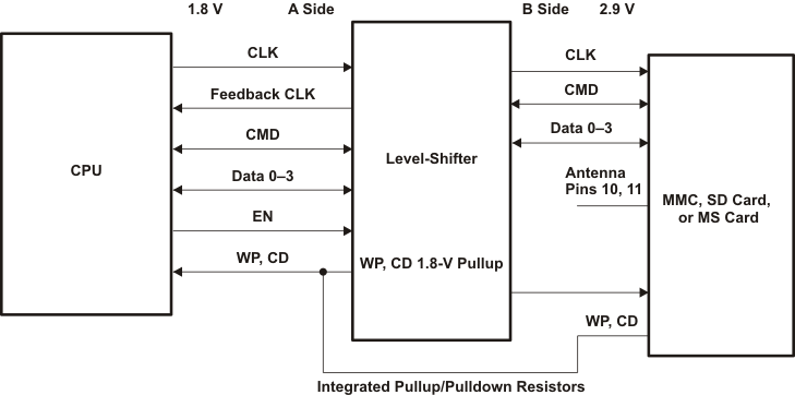 Figure 5. Typical Application Circuit
9.2.1 Design Requirements
For this design example, use the parameters listed in Table 2
Table 2. Design Parameters
| PARAMETERS | VALUES |
|---|---|
| Input voltage | 1.1 V to 3.6 V |
| Output voltage | 1.1 V to 3.6 V |
9.2.2 Detailed Design Procedure
To begin the design process, determine the following:
- Input voltage range
- Use the supply voltage of the microprocessor that is driving the TXS0206A to determine the input voltage range. For a valid logic high, the value must exceed the VIH of the input port. For a valid logic low, the value must be less than the VIL of the input port.
- Output voltage range
- Use the supply voltage of the memory card that the TXS0206A is driving to determine the output voltage range.
9.2.2.1 External Pulldown Resistors
When using the TXS0206A device with MMCs, SD, and Memory Stick™ to ensure that a valid receiver input voltage high (VIH) is achieved, the value of any pulldown resistors (external or internal to a memory card) must not be smaller than a 10-kΩ value. The impact of adding too heavy (less than 10-kΩ value) a pulldown resistor to the data and command lines of the TXS0206A device and the resulting 4-kΩ pullup / 10-kΩ pulldown voltage divider network has a direct impact on the VIH of the signal being sent into the memory card and its associated logic.
The resulting VIH voltage for the 10-kΩ pulldown resistor value would be:
VCC × 10 kΩ / (10 kΩ+ 4 kΩ) = 0.714 × VCC
This is marginally above a valid input high voltage for a 1.8-V signal (i.e., 0.65 × VCC).
The resulting VIH voltage for 20-kΩ pulldown resistor value would be:
VCC × 20 kΩ / (20 kΩ + 4 kΩ) = 0.833 × VCC
Which is above the valid input high voltage for a 1.8-V signal of 0.65 × VCC.
9.2.3 Application Curves
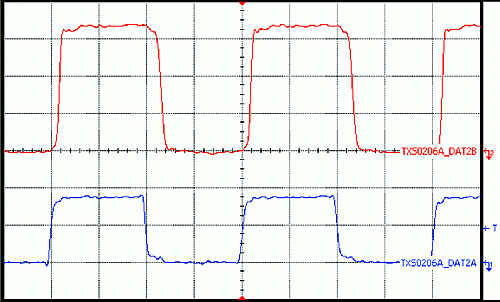 Figure 6. 1.8 V to 3.3 V Translation at 25 MHz
9.3 System Examples
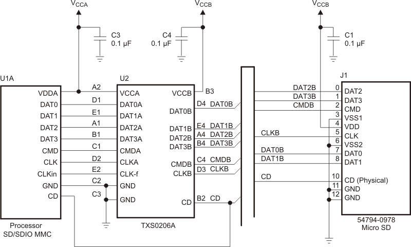 Figure 7. Interfacing With SD/SDIO Card
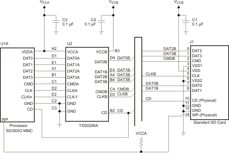 Figure 8. Interfacing With Seperate WP and CD Pin
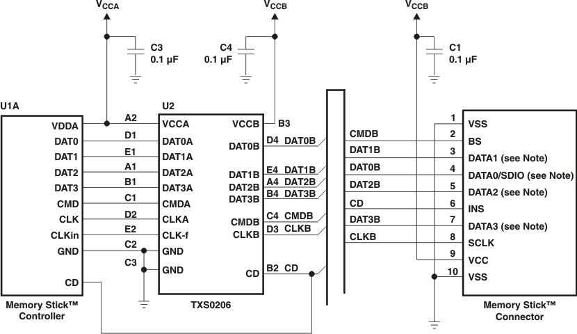 Figure 9. Interfacing With Memory Stick™ Card