SCES940A February 2022 – May 2024 TXU0101
PRODMIX
- 1
- 1 Features
- 2 Applications
- 3 Description
- 4 Pin Configuration and Functions—TXU0101
-
5 Specifications
- 5.1 Absolute Maximum Ratings
- 5.2 ESD Ratings
- 5.3 Recommended Operating Conditions
- 5.4 Thermal Information
- 5.5 Electrical Characteristics
- 5.6 Switching Characteristics, VCCA = 1.2 ± 0.1V
- 5.7 Switching Characteristics, VCCA = 1.5 ± 0.1V
- 5.8 Switching Characteristics, VCCA = 1.8 ± 0.15V
- 5.9 Switching Characteristics, VCCA = 2.5 ± 0.2V
- 5.10 Switching Characteristics, VCCA = 3.3 ± 0.3V
- 5.11 Switching Characteristics, VCCA = 5.0 ± 0.5V
- 5.12 Operating Characteristics
- 5.13 Typical Characteristics
- 6 Parameter Measurement Information
-
7 Detailed Description
- 7.1 Overview
- 7.2 Functional Block Diagram
- 7.3
Feature Description
- 7.3.1 CMOS Schmitt-Trigger Inputs with Integrated Pulldowns
- 7.3.2 Control Logic (OE) with VCC(MIN) Circuitry
- 7.3.3 Balanced High-Drive CMOS Push-Pull Outputs
- 7.3.4 VCC Isolation and VCC Disconnect
- 7.3.5 Over-Voltage Tolerant Inputs
- 7.3.6 Glitch-Free Power Supply Sequencing
- 7.3.7 Negative Clamping Diodes
- 7.3.8 Fully Configurable Dual-Rail Design
- 7.3.9 Supports High-Speed Translation
- 7.4 Device Functional Modes
- 8 Application and Implementation
- 9 Device and Documentation Support
- 10Revision History
- 11Mechanical, Packaging, and Orderable Information
Package Options
Refer to the PDF data sheet for device specific package drawings
Mechanical Data (Package|Pins)
- DBV|6
- DTQ|6
- DCK|6
- DRY|6
Thermal pad, mechanical data (Package|Pins)
- DRY|6
Orderable Information
3 Description
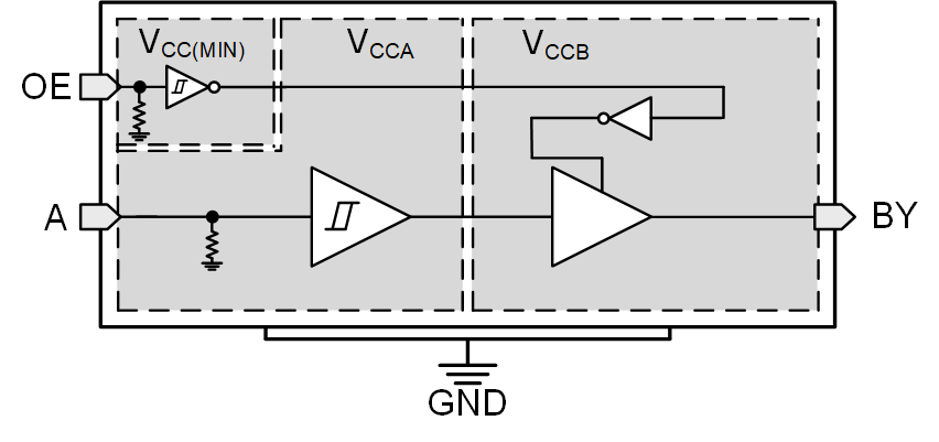
TXU0101 is a 1-bit, dual-supply noninverting fixed direction voltage level translation device. A pin is referenced to VCCA logic level, OE pin can be referenced to either VCCA or VCCB logic levels, and B pin is referenced to VCCB logic level. The A port is able to accept input voltages ranging from 1.1V to 5.5V, while the B port can also accept input voltages from 1.1V to 5.5V. Fixed direction data transmission can occur from A to B when OE is set to high in reference to either supply. When OE is set to low, all output pins are in the high-impedance state. See Device Functional Modes for a summary of the operation of the control logic.
| PART NUMBER | PACKAGE(1) | PACKAGE SIZE(2) |
|---|---|---|
| TXU0101 | DBV (SOT-23, 6) | 2.9mm × 2.8mm |
| DCK (SC70, 6) | 2mm × 2.1mm | |
| DRL (SOT-5X3, 6)(3) | 1.6mm × 1.6mm | |
| DRY (SON, 6) | 1.45mm × 1mm | |
| DTQ (X2SON, 6) | 1mm × 0.8mm |
 TXU0101 Functional Block Diagram