SCES930B April 2021 – March 2022 TXU0104-Q1
PRODUCTION DATA
- 1 Features
- 2 Applications
- 3 Description
- 4 Revision History
- 5 Related Products
- 6 Pin Configuration and Functions—TXU0104-Q1
-
7 Specifications
- 7.1 Absolute Maximum Ratings
- 7.2 ESD Ratings
- 7.3 Recommended Operating Conditions
- 7.4 Thermal Information
- 7.5 Electrical Characteristics
- 7.6 Switching Characteristics: Tsk, TMAX
- 7.7 Switching Characteristics, VCCA = 1.2 ± 0.1 V
- 7.8 Switching Characteristics, VCCA = 1.5 ± 0.1 V
- 7.9 Switching Characteristics, VCCA = 1.8 ± 0.15 V
- 7.10 Switching Characteristics, VCCA = 2.5 ± 0.2 V
- 7.11 Switching Characteristics, VCCA = 3.3 ± 0.3 V
- 7.12 Switching Characteristics, VCCA = 5.0 ± 0.5 V
- 7.13 Operating Characteristics
- 7.14 Typical Characteristics
- 8 Parameter Measurement Information
-
9 Detailed Description
- 9.1 Overview
- 9.2 Functional Block Diagram
- 9.3
Feature Description
- 9.3.1 CMOS Schmitt-Trigger Inputs with Integrated Pulldowns
- 9.3.2 Control Logic (OE) with VCC(MIN) Circuitry
- 9.3.3 Balanced High-Drive CMOS Push-Pull Outputs
- 9.3.4 Partial Power Down (Ioff)
- 9.3.5 VCC Isolation and VCC Disconnect
- 9.3.6 Over-Voltage Tolerant Inputs
- 9.3.7 Glitch-Free Power Supply Sequencing
- 9.3.8 Negative Clamping Diodes
- 9.3.9 Fully Configurable Dual-Rail Design
- 9.3.10 Supports High-Speed Translation
- 9.3.11 Wettable Flanks
- 9.4 Device Functional Modes
- 10Application and Implementation
- 11Power Supply Recommendations
- 12Layout
- 13Device and Documentation Support
- 14Mechanical, Packaging, and Orderable Information
Package Options
Mechanical Data (Package|Pins)
Thermal pad, mechanical data (Package|Pins)
- BQA|14
Orderable Information
9.3.8 Negative Clamping Diodes
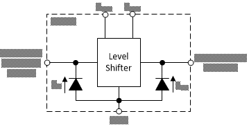
Figure 9-2 depicts the inputs and outputs to this device that have negative clamping diodes.
CAUTION:
Voltages beyond the values specified in the Absoulte Maximum Ratings table can cause damage to the device. The input negative-voltage and output voltage ratings may be exceeded if the input and output clamp-current ratings are observed.
 Figure 9-2 Electrical Placement of
Clamping Diodes for Each Input and Output