SLVS059U June   1976  – May 2024

PRODUCTION DATA  

  1.   1
  2. Features
  3. Applications
  4. Description
  5. Pin Configuration and Functions
  6. Specifications
    1. 5.1  Absolute Maximum Ratings
    2. 5.2  ESD Ratings
    3. 5.3  Recommended Operating Conditions
    4. 5.4  Thermal Information
    5. 5.5  Electrical Characteristics: UA78M33 (Both Legacy and New Chip)
    6. 5.6  Electrical Characteristics: UA78M05 (Both Legacy and New Chip)
    7. 5.7  Electrical Characteristics: UA78M06C (Legacy Chip Only)
    8. 5.8  Electrical Characteristics: UA78M08C (Legacy Chip Only)
    9. 5.9  Electrical Characteristics: UA78M09 (Legacy Chip Only)
    10. 5.10 Electrical Characteristics: UA78M10 (Legacy Chip Only)
    11. 5.11 Electrical Characteristics: UA78M12 (Legacy Chip Only)
    12. 5.12 Typical Characteristics
  7. Detailed Description
    1. 6.1 Overview
    2. 6.2 Functional Block Diagram
    3. 6.3 Feature Description
      1. 6.3.1 Current Limit
      2. 6.3.2 Dropout Voltage (VDO)
      3. 6.3.3 Thermal Shutdown
    4. 6.4 Device Functional Modes
      1. 6.4.1 Normal Operation
      2. 6.4.2 Dropout Operation
  8. Application and Implementation
    1. 7.1 Application Information
    2. 7.2 Typical Application
      1. 7.2.1 Design Requirements
      2. 7.2.2 Detailed Design Procedure
        1. 7.2.2.1 Input and Output Capacitor Requirements
        2. 7.2.2.2 Power Dissipation (PD)
        3. 7.2.2.3 Estimating Junction Temperature
        4. 7.2.2.4 External Capacitor Requirements
        5. 7.2.2.5 Overload Recovery
        6. 7.2.2.6 Reverse Current
        7. 7.2.2.7 Polarity Reversal Protection
      3. 7.2.3 Application Curves
    3. 7.3 System Examples
      1. 7.3.1 Positive Regulator in Negative Configuration
      2. 7.3.2 Current Limiter Circuit
    4. 7.4 Power Supply Recommendations
    5. 7.5 Layout
      1. 7.5.1 Layout Guidelines
      2. 7.5.2 Layout Example
  9. Device and Documentation Support
    1. 8.1 Device Support
      1. 8.1.1 Development Support
        1. 8.1.1.1 Evaluation Module
      2. 8.1.2 Device Nomenclature
    2. 8.2 Receiving Notification of Documentation Updates
    3. 8.3 Support Resources
    4. 8.4 Trademarks
    5. 8.5 Electrostatic Discharge Caution
    6. 8.6 Glossary
  10. Revision History
  11. 10Mechanical, Packaging, and Orderable Information

Package Options

Refer to the PDF data sheet for device specific package drawings

Mechanical Data (Package|Pins)
  • KVU|3
  • DCY|4
  • KCS|3
Thermal pad, mechanical data (Package|Pins)
Orderable Information

Application Curves

uA78M VIN vs
                            VOUT at TJ = 25°C (Legacy Chip)
VOUT = 5V
Figure 7-4 VIN vs VOUT at TJ = 25°C (Legacy Chip)
uA78M VIN vs
                            VOUT at TJ = 25°C (New Chip)
VOUT = 3.3V
Figure 7-6 VIN vs VOUT at TJ = 25°C (New Chip)
uA78M Load Transient Behavior (New
                        Chip)
VIN = 10V, VOUT = 5V, IOUT = 1mA to 100mA, dI/dt = 1A/μs, COUT = 0.1μF
Figure 7-8 Load Transient Behavior (New Chip)
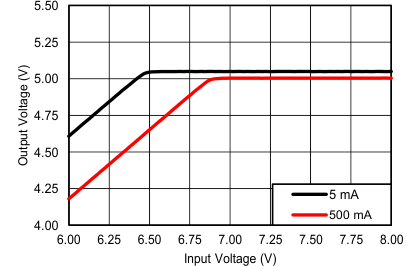
uA78M VIN vs VOUT at
                        TJ = 25°C (New Chip)
VOUT = 5V
Figure 7-5 VIN vs VOUT at TJ = 25°C (New Chip)
uA78M Line
                        Transient Behavior (New Chip)
VO = 5V, dVIN/dt = 1V/μs, IOUT = 350mA, COUT = 0.1μF
Figure 7-7 Line Transient Behavior (New Chip)
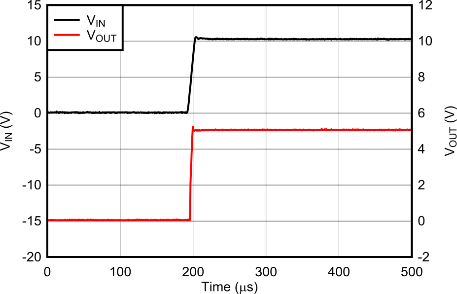
uA78M Start-Up (New Chip)
VIN = 0V to 10V, VOUT = 5V, IOUT = 100mA, dVIN/dt = 1V/μs, COUT = 0.1μF
Figure 7-9 Start-Up (New Chip)