SLUS191D February 1997 – July 2017 UC1525A , UC1527A , UC2525A , UC2527A , UC3525A , UC3527A
PRODUCTION DATA.
- 1 Features
- 2 Applications
- 3 Description
- 4 Revision History
- 5 Pin Configuration and Functions
- 6 Specifications
- 7 Detailed Description
- 8 Application and Implementation
- 9 Power Supply Recommendations
- 10Layout
- 11Device and Documentation Support
- 12Mechanical, Packaging, and Orderable Information
Package Options
Refer to the PDF data sheet for device specific package drawings
Mechanical Data (Package|Pins)
- J|16
- FK|20
Thermal pad, mechanical data (Package|Pins)
Orderable Information
8 Application and Implementation
NOTE
Information in the following applications sections is not part of the TI component specification, and TI does not warrant its accuracy or completeness. TI’s customers are responsible for determining suitability of components for their purposes. Customers should validate and test their design implementation to confirm system functionality.
8.1 Application Information
The UC1525A/1527A series of pulse width modulator integrated circuits are designed to offer improved performance and lowered external parts count when used in designing all types of switching power supplies. The UC1525A output stage features NOR logic, giving a LOW output for an OFF state. The UC1527A utilizes OR logic which results in a HIGH output level when OFF.
8.2 Typical Application
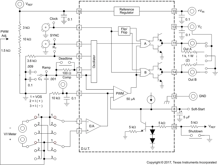 Figure 5. Lab Test Fixture
8.2.1 Theory of Operation
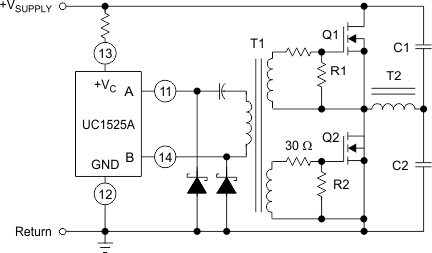 Figure 6. Low Power Transformers
Low power transformers can be driven by the UC1525A. Automatic reset occurs during dead time, when both ends of the primary winding are switched to ground.
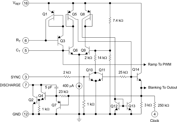 Figure 7. UC1525A Oscillator Schematic
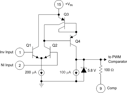 Figure 8. UC1525A Error Amplifier
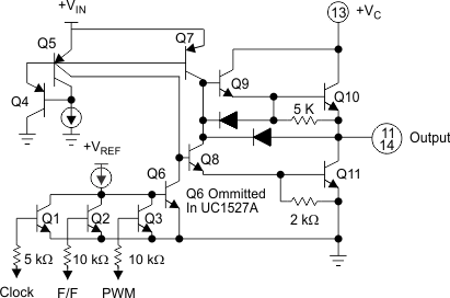 Figure 9. UC1525A Output Circuit (1/2 circuit shown)
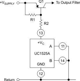 Figure 10. Grounded Driver Outputs For Single-Ended Supplies
For single-ended supplies, the driver outputs are grounded. The VC terminal is switched to ground by the totem-pole source transistors on alternate oscillator cycles.
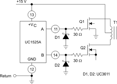 Figure 11. Output Drivers With Low Source Impedance
The low source impedance of the output drivers provides rapid charging of power FET input capacitance while minimizing external components.
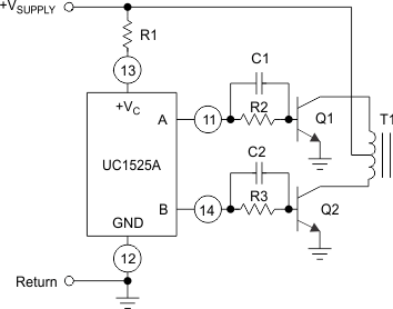 Figure 12. Conventional Push-Pull Bipolar Design
In conventional push-pull bipolar designs, forward base drive is controlled by R1–R3. Rapid turn-off times for the power devices are achieved with speed-up capacitors C1 and C2.
8.2.2 Design Requirements
This example illustrates the design process and component selection for a push-pull DC-DC converter utilizing the UC1525A. The converter regulates a 30-V input to a 5-V output with 10-A maximum load.
Table 1. Design Parameters
| PARAMETER | MIN | TYP | MAX | UNIT | |
|---|---|---|---|---|---|
| VIN | Input voltage range | 25 | 30 | 35 | V |
| VOUT | Output voltage | 5 | V | ||
| iOUT | Output current | 1 | 10 | A | |
| fO | Oscillator frequency | 100 | kHz | ||
| fS | Switching frequency | 50 | kHz | ||
8.2.3 Detailed Design Procedure
8.2.3.1 Timing Resistor and Capacitor Selection
Generally, higher switching frequency gives smaller size but have higher switching loss. Operation at 100 kHz was selected in this example as a reasonable compromise between size and efficiency. The value of RT = 10 kΩ, CT = 1.37 nF and RD = 100 Ω were chosen for 100-kHz oscillator frequency based on equation:

8.2.3.2 Turns Ratio Selection
The maximum primary-to-secondary turns ratio NMAX can be determined by the target output voltage, minimum input voltage, and the estimated maximum duty cycle. DLIM = 0.35 was selected for this example. NMAX can be calculated using Equation 1.

Rounding NMAX down to the next lowest integer results in a turns ratio of N = 3.
8.2.3.3 Inductor Selection
The maximum inductor ripple current occurs at the maximum input voltage. Typically, 20% to 40% of the full load current ripple is a good compromise between core loss and copper loss of the inductor. Higher ripple current allows for a smaller inductor size, but places more burden on the output capacitor to smooth the ripple voltage on the output. In this example, a ripple current of 25% of 10 A was chosen. The inductor value can be calculated as:

8.2.3.4 Rectification Diode Selection
A rectification diode should always possess low-forward voltage drop. When used in high-frequency switching applications, the diode must also possess a short recovery time. Schottky diodes meet both requirements and are therefore strongly recommended in push-pull converter designs.
8.2.3.5 VC Capacitor Selection
The primary purpose of the VC capacitor is to supply the peak transient currents of the drivers as well as provide stability for the VC regulator. These peak currents can be several amperes. The recommended value of VC capacitor should be no smaller than 0.1 μF, and should be a good quality, low ESR, ceramic capacitor. VC capacitor should be placed as close as possible to the VC pin to minimize potentially damaging voltage transients caused by trace inductance.
8.2.3.6 Output Capacitor Selection
The output capacitors smooth the output voltage ripple caused by inductor ripple current and provide a source of charge during load transient conditions.
8.2.3.7 Input Capacitor Selection
The input supply voltage typically has high source impedance at the switching frequency. Good quality input capacitors are necessary to limit the ripple voltage at the VIN pin while supplying most of the switch current during the on-time. The input capacitor should be selected for RMS current rating and minimum ripple voltage.
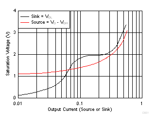
8.2.4 Application Curves
