SLUS191D February   1997  – July 2017 UC1525A , UC1527A , UC2525A , UC2527A , UC3525A , UC3527A

PRODUCTION DATA.  

  1. Features
  2. Applications
  3. Description
  4. Revision History
  5. Pin Configuration and Functions
  6. Specifications
    1. 6.1 Absolute Maximum Ratings
    2. 6.2 ESD Ratings
    3. 6.3 Recommended Operating Conditions
    4. 6.4 Thermal Information
    5. 6.5 Electrical Characteristics
    6. 6.6 Typical Characteristics
  7. Detailed Description
    1. 7.1 Overview
    2. 7.2 Functional Block Diagram
    3. 7.3 Feature Description
      1. 7.3.1 Adjustable Dead-Time Control
      2. 7.3.2 Soft Start
      3. 7.3.3 Input Undervoltage Lockout With Hysteresis
      4. 7.3.4 Shutdown and Pulse-by-Pulse Current Limiting
    4. 7.4 Device Functional Modes
      1. 7.4.1 Shutdown Options (See )
  8. Application and Implementation
    1. 8.1 Application Information
    2. 8.2 Typical Application
      1. 8.2.1 Theory of Operation
      2. 8.2.2 Design Requirements
      3. 8.2.3 Detailed Design Procedure
        1. 8.2.3.1 Timing Resistor and Capacitor Selection
        2. 8.2.3.2 Turns Ratio Selection
        3. 8.2.3.3 Inductor Selection
        4. 8.2.3.4 Rectification Diode Selection
        5. 8.2.3.5 VC Capacitor Selection
        6. 8.2.3.6 Output Capacitor Selection
        7. 8.2.3.7 Input Capacitor Selection
      4. 8.2.4 Application Curves
  9. Power Supply Recommendations
  10. 10Layout
    1. 10.1 Layout Guidelines
    2. 10.2 Layout Example
  11. 11Device and Documentation Support
    1. 11.1 Documentation Support
      1. 11.1.1 Related Documentation
    2. 11.2 Related Links
    3. 11.3 Community Resources
    4. 11.4 Trademarks
    5. 11.5 Electrostatic Discharge Caution
    6. 11.6 Glossary
  12. 12Mechanical, Packaging, and Orderable Information

Package Options

Refer to the PDF data sheet for device specific package drawings

Mechanical Data (Package|Pins)
  • J|16
  • FK|20
Thermal pad, mechanical data (Package|Pins)
Orderable Information

Layout

Layout Guidelines

High-speed circuits demand careful attention to layout and component placement. To assure proper performance of the UC1525A follow these rules:

  • Use a ground plane
  • Damp or clamp parasitic inductive kick energy from the gate of driven MOSFETs. Do not allow the output pins to ring below ground. A series gate resistor or a shunt 1-A Schottky diode at the output pin will serve this purpose.
  • Bypass VIN, VC, and VREF. Use 0.1-µF monolithic ceramic capacitors with low equivalent series inductance. Allow less than 1 cm of total lead length for each capacitor between the bypassed pin and the ground plane.
  • Treat the timing capacitor, CT, like a bypass capacitor.

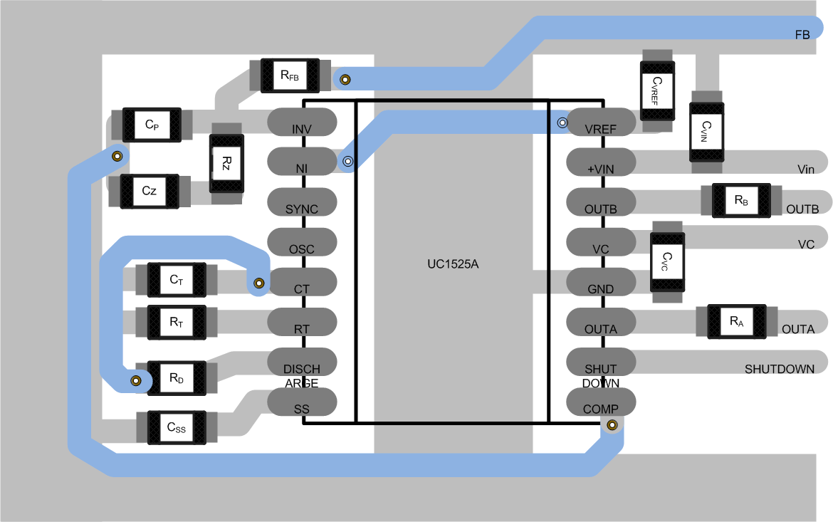
Layout Example

UC1525A UC1527A UC2525A UC2527A UC3525A UC3527A layout_lus191.gif Figure 14. UC1525A Layout Example