SLUSAG0A March 2011 – March 2016 UC1707-SP
PRODUCTION DATA.
- 1 Features
- 2 Applications
- 3 Description
- 4 Revision History
- 5 Pin Configuration and Functions
- 6 Specifications
- 7 Parameter Measurement Information
- 8 Detailed Description
- 9 Application and Implementation
- 10Power Supply Recommendations
- 11Layout
- 12Device and Documentation Support
- 13Mechanical, Packaging, and Orderable Information
Package Options
Mechanical Data (Package|Pins)
Thermal pad, mechanical data (Package|Pins)
Orderable Information
9 Application and Implementation
NOTE
Information in the following applications sections is not part of the TI component specification, and TI does not warrant its accuracy or completeness. TI’s customers are responsible for determining suitability of components for their purposes. Customers should validate and test their design implementation to confirm system functionality.
9.1 Application Information
UC1707-SP MOSFET driver IC is designed to provide fast transition and high peak currents required for the MOSFETs. Each driver features TTL compatible input thresholds, undervoltage lockout, thermal shutdown and low cross conduction, high-speed output circuitry. The peak current of each totem-pole output, whether source or sink is 1.5 A. However, on dual output versions as in UC1707-SP both of the outputs can be paralleled for 3-A peak current.
9.2 Typical Application
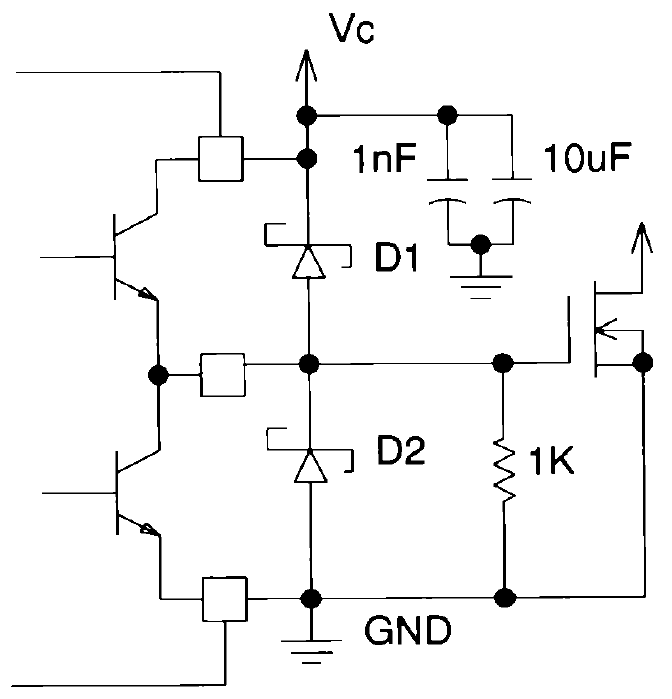 Figure 13. Power MOSFET Drive Circuit
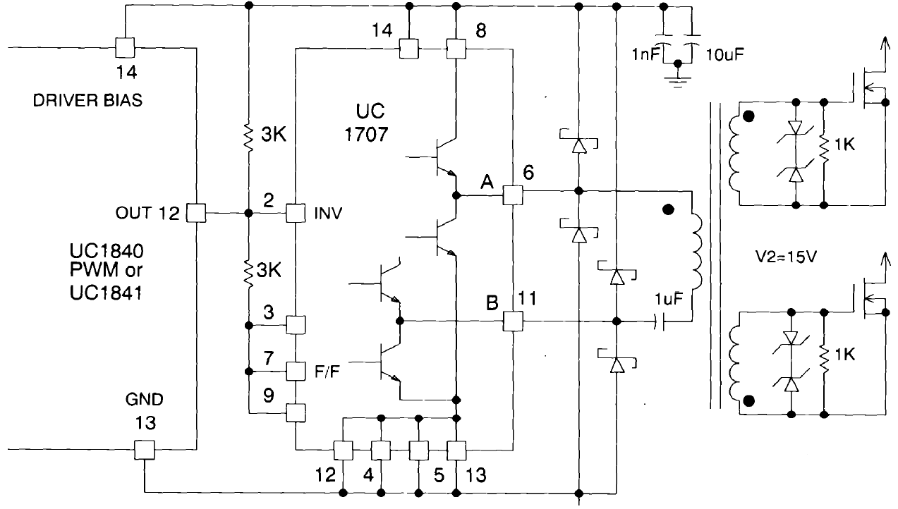 Figure 14. Convert Single Output PWMS High-Current Push-Pull Configuration
9.2.1 Design Requirements
Push-Pull Transformer coupling – driving MOSFETs with transformer coupled winding.
9.2.2 Detailed Design Procedure
The totem-pole outputs of the UC1707-SP can easily be configured for implementing the balanced transformer drive as shown in Figure 14. Output A and B are alternating now as the internal flip-flop is active and the output frequency is halved. When the UC1707-SP output goes high, the other is held low during the dead time between output pulses. With balanced operation, no coupling capacitor on the primary is necessary since there is no net DC in the primary. Schottky clamp diodes on the primary side and back to back Zener diodes on the secondary are necessary to minimize the overshoot caused by the ringing of the gate capacitance with circuit inductances.
9.2.3 Application Curves
t = 1 µs/DIV.The following waveforms refer to the application in Figure 14.
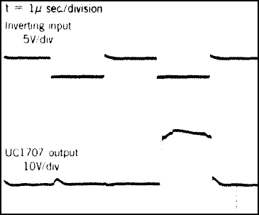 Figure 15. Inverting Input and UC1707 Output
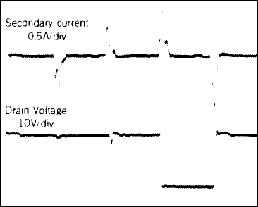 Figure 17. Secondary Current and Drain Voltage
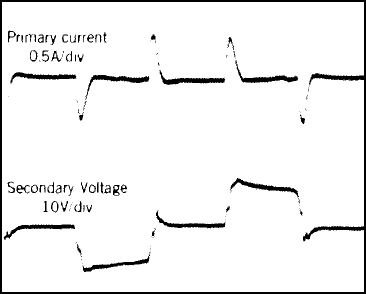 Figure 16. Primary Current and Secondary Voltage