SLUSAG0A March 2011 – March 2016 UC1707-SP
PRODUCTION DATA.
- 1 Features
- 2 Applications
- 3 Description
- 4 Revision History
- 5 Pin Configuration and Functions
- 6 Specifications
- 7 Parameter Measurement Information
- 8 Detailed Description
- 9 Application and Implementation
- 10Power Supply Recommendations
- 11Layout
- 12Device and Documentation Support
- 13Mechanical, Packaging, and Orderable Information
Package Options
Mechanical Data (Package|Pins)
Thermal pad, mechanical data (Package|Pins)
Orderable Information
11 Layout
11.1 Layout Guidelines
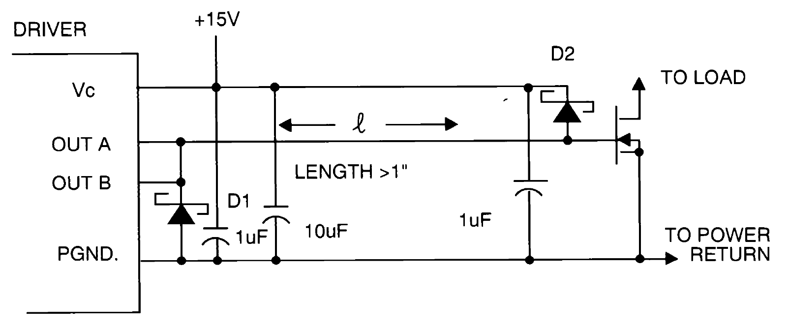
Directly connecting the MOSFET gate to the output of the driver is straighforward for testing purposes. It does not represent the "real" application which may include several inches of printed circuit board traces. Inductance will sharply degrade the transitions and cause substantial overshoot by ringing with the gate capacitance. This can cause the gate-to-source voltage to overshoot beyond the specified maximum ratings. Additionally, negative transitions (below ground) at the driver output can raise havoc with the internal circuitry, leading to undesirable performance.
Adding Schottky diodes to auxiliary supply rail can help address these concerns.
11.2 Layout Example
 Figure 18. Layout