SLUS873C January 2009 – December 2016 UC1825A-SP
PRODUCTION DATA.
- 1 Features
- 2 Applications
- 3 Description
- 4 Revision History
- 5 Description (continued)
- 6 Pin Configuration and Functions
- 7 Specifications
- 8 Detailed Description
-
9 Application and Implementation
- 9.1 Application Information
- 9.2
Typical Application
- 9.2.1 Design Requirements
- 9.2.2
Detailed Design Procedure
- 9.2.2.1 Auxiliary Supply Voltage
- 9.2.2.2 Oscillator Frequency
- 9.2.2.3 Preliminary Considerations
- 9.2.2.4 Input Power
- 9.2.2.5 Primary Current
- 9.2.2.6 Sense Resistor R(s)
- 9.2.2.7 MOSFET DC Losses
- 9.2.2.8 Selection of Core Material
- 9.2.2.9 Main Transformer Design
- 9.2.2.10 Calculation of Transformer
- 9.2.2.11 Minimum Core Size
- 9.2.2.12 Core Loss Limited Conditions
- 9.2.2.13 Core Geometry Selection
- 9.2.2.14 Wire Size Selection
- 9.2.2.15 Calculate Secondary RMS Current
- 9.2.2.16 Transformer Assembly
- 9.2.2.17 Calculation of Winding Resistances and Losses
- 9.2.2.18 Transformer Power Losses
- 9.2.2.19 Output Section
- 9.2.2.20 UC1825A-SP PWM Control Section
- 9.2.2.21 Closing the Feedback Loop
- 9.2.2.22 Summary
- 9.2.3 Application Curves
- 10Power Supply Recommendations
- 11Layout
- 12Device and Documentation Support
- 13Mechanical, Packaging, and Orderable Information
Package Options
Mechanical Data (Package|Pins)
Thermal pad, mechanical data (Package|Pins)
Orderable Information
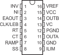
6 Pin Configuration and Functions
J Package
16-Pin CDIP
Top View

HKT Package
16-Pin CFP
Top View
Pin Functions
| PIN | I/O | DESCRIPTION | |
|---|---|---|---|
| NAME | NO. | ||
| CLK/LEB | 4 | O | Output of the internal oscillator. |
| CT | 6 | I | Timing capacitor connection pin for oscillator frequency programming. The timing capacitor must be connected to the device ground using minimal trace length. |
| EAOUT | 3 | O | Output of the error amplifier for compensation. |
| GND | 10 | — | Analog ground return pin. |
| ILIM | 9 | I | Input to the current limit comparator. |
| INV | 1 | I | Inverting input to the error amplifier. |
| NI | 2 | I | Noninverting input to the error amplifier. |
| OUTA | 11 | O | High current totem pole output A of the on-chip drive stage. |
| OUTB | 14 | O | High current totem pole output B of the on-chip drive stage. |
| PGND | 12 | — | Ground return pin for the output driver stage. |
| RAMP | 7 | I | Noninverting input to the PWM comparator with 1.25-V internal input offset. In voltage mode operation, this serves as the input voltage feed-forward function by using the CT ramp. In peak current mode operation, this serves as the slope compensation input. |
| RT | 5 | I | Timing resistor connection pin for oscillator frequency programming. |
| SS | 8 | I | Soft-start input pin that also doubles as the maximum duty cycle clamp. |
| VC | 13 | — | Power supply pin for the output stage. This pin must be bypassed with a 0.1-μF monolithic ceramic low ESL capacitor with minimal trace lengths. |
| VCC | 15 | — | Power supply pin for the device. This pin must be bypassed with a 0.1-μF monolithic ceramic low ESL capacitor with minimal trace lengths. |
| VREF | 16 | O | 5.1-V reference. For stability, the reference must be bypassed with a 0.1-μF monolithic ceramic low ESL capacitor and minimal trace length to the ground plane. |