SLUS334F August 1995 – August 2022 UC1823A , UC1825A , UC2823A , UC2823B , UC2825A , UC2825B , UC3823A , UC3823B , UC3825A , UC3825B
PRODUCTION DATA
- 1Features
- 2Description
- 3Revision History
- 4Ordering Information
- 5Pin Configuration and Functions
- 6Specifications
- 7Application and Implementation
- 8Device and Documentation Support
- 9Mechanical, Packaging, and Orderable Information
Package Options
Refer to the PDF data sheet for device specific package drawings
Mechanical Data (Package|Pins)
- J|16
- FK|20
Thermal pad, mechanical data (Package|Pins)
Orderable Information
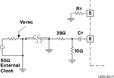
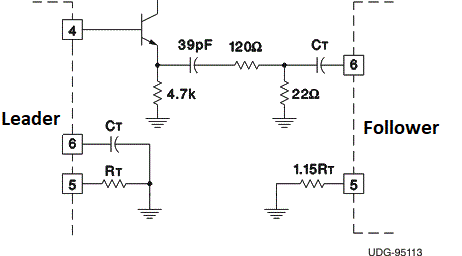
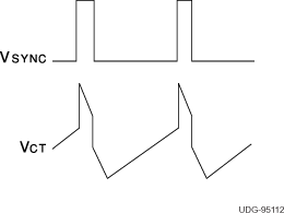
7.5 SYNCHRONIZATION
The oscillator can be synchronized by an external pulse inserted in series with the timing capacitor. Program the free running frequency of the oscillator to be 10% to 15% slower than the desired synchronous frequency. The pulse width should be greater than 10 ns and less than half the discharge time of the oscillator. The rising edge of the CLK/LEB pin can be used to generate a synchronizing pulse for other chips. Note that the CLK/LEB pin no longer accepts an incoming synchronizing signal.
 Figure 7-6 General Oscillator Synchronization
 Figure 7-7 Two Unit Interface
 Figure 7-8 Operational Waveforms