SLUS334F August 1995 – August 2022 UC1823A , UC1825A , UC2823A , UC2823B , UC2825A , UC2825B , UC3823A , UC3823B , UC3825A , UC3825B
PRODUCTION DATA
- 1Features
- 2Description
- 3Revision History
- 4Ordering Information
- 5Pin Configuration and Functions
- 6Specifications
- 7Application and Implementation
- 8Device and Documentation Support
- 9Mechanical, Packaging, and Orderable Information
Package Options
Refer to the PDF data sheet for device specific package drawings
Mechanical Data (Package|Pins)
- J|16
- FK|20
Thermal pad, mechanical data (Package|Pins)
Orderable Information
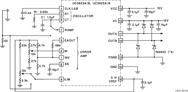
7.8 OPEN LOOP TEST CIRCUIT
This test fixture is useful for exercising many functions of this device family and measuring their specifications. As with any wideband circuit, careful grounding and bypass procedures should be followed. The use of a ground plane is highly recommended.
 Figure 7-11 Open Loop Test Circuit Schematic