SLUS334F August 1995 – August 2022 UC1823A , UC1825A , UC2823A , UC2823B , UC2825A , UC2825B , UC3823A , UC3823B , UC3825A , UC3825B
PRODUCTION DATA
- 1Features
- 2Description
- 3Revision History
- 4Ordering Information
- 5Pin Configuration and Functions
- 6Specifications
- 7Application and Implementation
- 8Device and Documentation Support
- 9Mechanical, Packaging, and Orderable Information
Package Options
Refer to the PDF data sheet for device specific package drawings
Mechanical Data (Package|Pins)
- J|16
- FK|20
Thermal pad, mechanical data (Package|Pins)
Orderable Information
7.7 GROUND PLANES
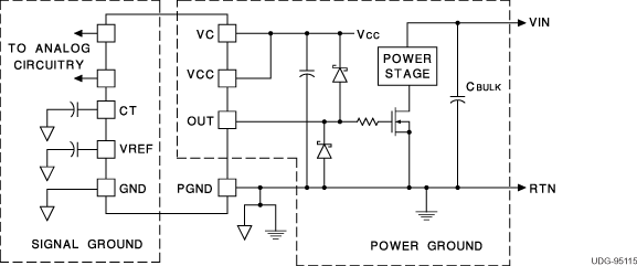
Each output driver of these devices is capable of 2-A peak currents. Careful layout is essential for correct operation of the chip. A ground plane must be employed. A unique section of the ground plane must be designated for high di/dt currents associated with the output stages. This point is the power ground to which the PGND pin is connected. Power ground can be separated from the rest of the ground plane and connected at a single point, although this is not necessary if the high di/dt paths are well understood and accounted for. VCC should be bypassed directly to power ground with a good high frequency capacitor. The sources of the power MOSFET should connect to power ground as should the return connection for input power to the system and the bulk input capacitor. The output should be clamped with a high current Schottky diode to both VCC and PGND. Nothing else should be connected to power ground.
VREF should be bypassed directly to the signal portion of the ground plane with a good high frequency capacitor. Low ESR/ESL ceramic 1-mF capacitors are recommended for both VCC and VREF. All analog circuitry should likewise be bypassed to the signal ground plane.
 Figure 7-10 Ground Planes Diagram