SLUS223H April 1997 – October 2024 UC1842 , UC1843 , UC1844 , UC1845 , UC2842 , UC2843 , UC2844 , UC2845 , UC3842 , UC3843 , UC3844 , UC3845
PRODUCTION DATA
- 1
- 1 Features
- 2 Applications
- 3 Description
- 4 Device Comparison Table
- 5 Pin Configuration and Functions
- 6 Specifications
-
7 Detailed Description
- 7.1 Overview
- 7.2 Functional Block Diagrams
- 7.3 Feature Description
- 7.4 Device Functional Modes
-
8 Application and Implementation
- 8.1 Application Information
- 8.2
Typical Application
- 8.2.1 Design Requirements
- 8.2.2
Detailed Design Procedure
- 8.2.2.1 Input Bulk Capacitor and Minimum Bulk Voltage
- 8.2.2.2 Transformer Turns Ratio and Maximum Duty Cycle
- 8.2.2.3 Transformer Inductance and Peak Currents
- 8.2.2.4 Output Capacitor
- 8.2.2.5 Current Sensing Network
- 8.2.2.6 Gate Drive Resistor
- 8.2.2.7 VREF Capacitor
- 8.2.2.8 RT/CT
- 8.2.2.9 Start-Up Circuit
- 8.2.2.10 Voltage Feedback Compensation
- 8.2.3 Application Curves
- 8.3 Power Supply Recommendations
- 8.4 Layout
- 9 Device and Documentation Support
- 10Revision History
- 11Mechanical, Packaging, and Orderable Information
Package Options
Mechanical Data (Package|Pins)
- JG|8
Thermal pad, mechanical data (Package|Pins)
Orderable Information
8.2.2.10.4 Compensation Loop
The design of the compensation loop involves selecting the appropriate components so that the required gain, poles, and zeros can be designed to result in a stable system over the entire operating range. There are three distinct portions of the loop: the TL431, the opto-coupler, and the error amplifier. Each of these stages is combined with the power stage to result in a stable robust system.
For good transient response, the bandwidth of the finalized design must be as large as possible. The bandwidth of a CCM flyback, fBW, is limited to ¼ of the RHP zero frequency, or approximately 1.77 kHz using Equation 47.

The gain of the open-loop power stage at fBW can be calculated using Equation 46 or can be observed on the Bode plot (Figure 8-3 ) and is equal to –19.55 dB and the phase at fBW is equal to –58°.
The secondary side portion of the compensation loop begins with establishing the regulated steady state output voltage. To set the regulated output voltage, a TL431 adjustable precision shunt regulator is ideally suited for use on the secondary side of isolated converters due to the accurate voltage reference and internal op amp. The resistors used in the divider from the output terminals of the converter to the TL431 REF pin are selected based upon the desired power consumption. Because the REF input current for the TL431 is only 2 µA, selecting the resistors for a divider current, IFB_REF, of 1 mA results in minimal error. The top divider resistor, RFBU, is calculated using Equation 48:

The TL431 reference voltage, REFTL431, has a typical value of 2.495 V. A 9.53-kΩ resistor is chosen for RFBU. To set the output voltage to 12 V, 2.49 kΩ is used for RFBB.

For good phase margin, a compensator zero, fCOMPz, is needed and must be placed at 1/10th the desired bandwidth:


With this converter, fCOMPz must be set at approximately 177 Hz. A series resistor, RCOMPz, and capacitor, CCOMPz, placed across the TL431 cathode to REF sets the compensator zero location. Setting CCOMPz to 0.01 µF, RCOMPz is calculated using Equation 52:

Using a standard value of 88.7 kΩ for RZ and a 0.01 µF for CZ results in a zero placed at 179 Hz.
Referring to Figure 8-2, RTLbias provides cathode current to the TL431 from the regulated voltage provided from the Zener diode, DREG. For robust performance, 10 mA is provided to bias the TL431 by way of the 10-V Zener and 1-kΩ resistor is used for RTLbias.
The gain of the TL431 portion of the compensation loop can be written as:

A compensation pole is needed at the frequency of right half plane zero or the ESR zero, whichever is lowest. Based previous the analysis, the right half plane zero, fRHPz, is located at 7.07 kHz and the ESR zero, fESRz, is at 1.68 kHz; therefore, for this design, the compensation pole must be put at 1.68 kHz. The opto-coupler contains a parasitic pole that is difficult to characterize over frequency so the opto-coupler is set up with a pulldown resistor, ROPTO equal to 1 kΩ, which moves the parasitic opto-coupler pole further out and beyond the range of interest for this design.
The required compensation pole can be added to the primary side error amplifier using RCOMPp and CCOMPp. Choosing RCOMPp as 10 kΩ, the required value of CCOMPp is determined using Equation 54.

A 10-nF capacitor is used for CCOMPp setting the compensation pole at 1.59 kHz.
Adding a DC gain to the primary side error amplifier can be required to obtain the required bandwidth and helps to adjust the loop gain as needed. Using a 4.99 kΩ for RFBG sets the DC gain on the error amplifier to 2. At this point the gain transfer function of the error amplifier stage, GEA(s), of the compensation loop can be characterized:

Using an opto-coupler whose current transfer ratio (CTR) is typically at 100% in the frequency range of interest so that CTR = 1, the transfer function of the opto-coupler stage, GOPTO(s), is equal to:

The bias resistor, RLED, to the internal diode of the opto-coupler, and the pulldown resistor on the opto emitter, ROPTO, sets the gain across the isolation boundary. ROPTO has already been set to 1 kΩ but the value of RLED has not yet been determined.
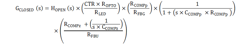
The total closed-loop gain, GTOTAL(s), is the combination of the open-loop power stage, Ho(s), the opto gain, GOPTO(s), the error amplifier gain, GEA(s), and the gain of the TL431 stage, GTL431(s):

The required value for RLED can be selected to achieve the desired crossover frequency, fBW. By setting the total loop gain equal to 1 at the desired crossover frequency and rearranging Equation 57, the optimal value for RLED can be determined, as shown in Equation 58.

A 1.3-kΩ resistor suits the requirement for RLED.
Based on the compensation loop structure, the entire compensation loop transfer function is written as Equation 59.
The final closed-loop bode plots are show in Figure 8-5 and Figure 8-6. The converter achieves a crossover frequency of approximately 1.8 kHz and has a phase margin of approximately 67o.
TI recommends checking the loop stability across all the corner cases including component tolerances to provide system stability.
 Figure 8-5 Converter Closed-Loop Bode Plot – Gain
 Figure 8-6 Converter Closed-Loop Bode Plot – Phase