SLUS223H April   1997  – October 2024 UC1842 , UC1843 , UC1844 , UC1845 , UC2842 , UC2843 , UC2844 , UC2845 , UC3842 , UC3843 , UC3844 , UC3845

PRODUCTION DATA  

  1.   1
  2. Features
  3. Applications
  4. Description
  5. Device Comparison Table
  6. Pin Configuration and Functions
  7. Specifications
    1. 6.1 Absolute Maximum Ratings
    2. 6.2 ESD Ratings
    3. 6.3 Recommended Operating Conditions
    4. 6.4 Thermal Information
    5. 6.5 Electrical Characteristics
    6. 6.6 Typical Characteristics
  8. Detailed Description
    1. 7.1 Overview
    2. 7.2 Functional Block Diagrams
    3. 7.3 Feature Description
      1. 7.3.1  Detailed Pin Description
        1. 7.3.1.1 COMP
        2. 7.3.1.2 VFB
        3. 7.3.1.3 ISENSE
        4. 7.3.1.4 RT/CT
        5. 7.3.1.5 GROUND
        6. 7.3.1.6 OUTPUT
        7. 7.3.1.7 VCC
        8. 7.3.1.8 VREF
      2. 7.3.2  Pulse-by-Pulse Current Limiting
      3. 7.3.3  Current-Sense
      4. 7.3.4  Error Amplifier With Low Output Resistance
      5. 7.3.5  Undervoltage Lockout
      6. 7.3.6  Oscillator
      7. 7.3.7  Synchronization
      8. 7.3.8  Shutdown Technique
      9. 7.3.9  Slope Compensation
      10. 7.3.10 Soft Start
      11. 7.3.11 Voltage Mode
    4. 7.4 Device Functional Modes
      1. 7.4.1 Normal Operation
      2. 7.4.2 UVLO Mode
  9. Application and Implementation
    1. 8.1 Application Information
      1. 8.1.1 Open-Loop Test Fixture
    2. 8.2 Typical Application
      1. 8.2.1 Design Requirements
      2. 8.2.2 Detailed Design Procedure
        1. 8.2.2.1  Input Bulk Capacitor and Minimum Bulk Voltage
        2. 8.2.2.2  Transformer Turns Ratio and Maximum Duty Cycle
        3. 8.2.2.3  Transformer Inductance and Peak Currents
        4. 8.2.2.4  Output Capacitor
        5. 8.2.2.5  Current Sensing Network
        6. 8.2.2.6  Gate Drive Resistor
        7. 8.2.2.7  VREF Capacitor
        8. 8.2.2.8  RT/CT
        9. 8.2.2.9  Start-Up Circuit
        10. 8.2.2.10 Voltage Feedback Compensation
          1. 8.2.2.10.1 Power Stage Poles and Zeroes
          2. 8.2.2.10.2 Slope Compensation
          3. 8.2.2.10.3 Open-Loop Gain
          4. 8.2.2.10.4 Compensation Loop
      3. 8.2.3 Application Curves
    3. 8.3 Power Supply Recommendations
    4. 8.4 Layout
      1. 8.4.1 Layout Guidelines
        1. 8.4.1.1 Feedback Traces
        2. 8.4.1.2 Bypass Capacitors
        3. 8.4.1.3 Compensation Components
        4. 8.4.1.4 Traces and Ground Planes
      2. 8.4.2 Layout Example
  10. Device and Documentation Support
    1. 9.1 Receiving Notification of Documentation Updates
    2. 9.2 Support Resources
    3. 9.3 Trademarks
    4. 9.4 Electrostatic Discharge Caution
    5. 9.5 Glossary
  11. 10Revision History
  12. 11Mechanical, Packaging, and Orderable Information

Package Options

Mechanical Data (Package|Pins)
Thermal pad, mechanical data (Package|Pins)
Orderable Information

Slope Compensation

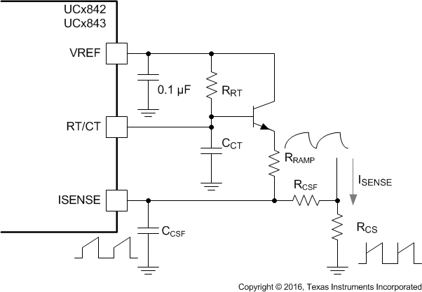
A fraction of the oscillator ramp can be summed resistively with the current-sense signal to provide slope compensation for converters requiring duty cycles over 50% (see Figure 7-11). Note that capacitor CCSF forms a filter with RCSF to suppress the leading-edge switch spikes.
UC1842 UC2842 UC3842 UC1843 UC2843 UC3843 UC1844 UC2844 UC3844 UC1845 UC2845 UC3845 Slope CompensationFigure 7-11 Slope Compensation