SLUS223H April 1997 – October 2024 UC1842 , UC1843 , UC1844 , UC1845 , UC2842 , UC2843 , UC2844 , UC2845 , UC3842 , UC3843 , UC3844 , UC3845
PRODUCTION DATA
- 1
- 1 Features
- 2 Applications
- 3 Description
- 4 Device Comparison Table
- 5 Pin Configuration and Functions
- 6 Specifications
-
7 Detailed Description
- 7.1 Overview
- 7.2 Functional Block Diagrams
- 7.3 Feature Description
- 7.4 Device Functional Modes
-
8 Application and Implementation
- 8.1 Application Information
- 8.2
Typical Application
- 8.2.1 Design Requirements
- 8.2.2
Detailed Design Procedure
- 8.2.2.1 Input Bulk Capacitor and Minimum Bulk Voltage
- 8.2.2.2 Transformer Turns Ratio and Maximum Duty Cycle
- 8.2.2.3 Transformer Inductance and Peak Currents
- 8.2.2.4 Output Capacitor
- 8.2.2.5 Current Sensing Network
- 8.2.2.6 Gate Drive Resistor
- 8.2.2.7 VREF Capacitor
- 8.2.2.8 RT/CT
- 8.2.2.9 Start-Up Circuit
- 8.2.2.10 Voltage Feedback Compensation
- 8.2.3 Application Curves
- 8.3 Power Supply Recommendations
- 8.4 Layout
- 9 Device and Documentation Support
- 10Revision History
- 11Mechanical, Packaging, and Orderable Information
Package Options
Mechanical Data (Package|Pins)
Thermal pad, mechanical data (Package|Pins)
Orderable Information
7.3.11 Voltage Mode
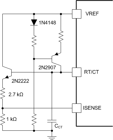
In duty cycle control (voltage mode), pulse width modulation is attained by comparing the error amplifier output to an artificial ramp. The oscillator timing capacitor CCT is used to generate a sawtooth waveform on both current or voltage mode ICs. To use the UCx84x in a voltage mode configuration, this sawtooth waveform is input to the current sense input, ISENSE, for comparison to the error voltage at the PWM comparator. This sawtooth is used to determine pulse width instead of the actual primary current in this method. Loop compensation is similar to that of voltage mode controllers with subtle differences due to the low output resistance voltage amplifier in the UCx84x as opposed to a transconductance (current) type amplifier used in traditional voltage mode controllers. For further reference on topologies and compensation, consult Closing the Feedback Loop (SLUP068).
 Figure 7-13 Current Mode PWM Used as a Voltage Mode PWM