SLUS223H April 1997 – October 2024 UC1842 , UC1843 , UC1844 , UC1845 , UC2842 , UC2843 , UC2844 , UC2845 , UC3842 , UC3843 , UC3844 , UC3845
PRODUCTION DATA
- 1
- 1 Features
- 2 Applications
- 3 Description
- 4 Device Comparison Table
- 5 Pin Configuration and Functions
- 6 Specifications
-
7 Detailed Description
- 7.1 Overview
- 7.2 Functional Block Diagrams
- 7.3 Feature Description
- 7.4 Device Functional Modes
-
8 Application and Implementation
- 8.1 Application Information
- 8.2
Typical Application
- 8.2.1 Design Requirements
- 8.2.2
Detailed Design Procedure
- 8.2.2.1 Input Bulk Capacitor and Minimum Bulk Voltage
- 8.2.2.2 Transformer Turns Ratio and Maximum Duty Cycle
- 8.2.2.3 Transformer Inductance and Peak Currents
- 8.2.2.4 Output Capacitor
- 8.2.2.5 Current Sensing Network
- 8.2.2.6 Gate Drive Resistor
- 8.2.2.7 VREF Capacitor
- 8.2.2.8 RT/CT
- 8.2.2.9 Start-Up Circuit
- 8.2.2.10 Voltage Feedback Compensation
- 8.2.3 Application Curves
- 8.3 Power Supply Recommendations
- 8.4 Layout
- 9 Device and Documentation Support
- 10Revision History
- 11Mechanical, Packaging, and Orderable Information
Package Options
Mechanical Data (Package|Pins)
Thermal pad, mechanical data (Package|Pins)
Orderable Information
7.3.4 Error Amplifier With Low Output Resistance
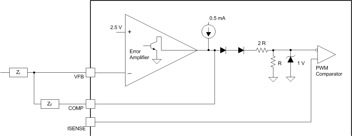
The error amplifier output is an open collector in parallel with a current source. With a low output resistance, various impedance networks can be used on the compensation pin input for error amplifier feedback. The error amplifier output, COMP, is frequently used as a control port for secondary-side regulation by using an external secondary-side adjustable voltage regulator, such as a TL431, to send an error signal across the secondary-to-primary isolation boundary through an opto-isolator, in this configuration connect the COMP pin directly to the opto-isolator feedback. On the primary side, the inverting input to the UCx48x error amplifier, VFB, must be connected to GROUND. With VFB tied to GROUND, the error amplifier output, COMP, is forced to the high state and sources current, typically 0.8 mA. The opto-isolator must overcome the source current capability to control the COMP pin below the error amplifier output high level, VOH.
For primary-side regulation, configure the inverting input to the error amplifier, VFB, with a resistor divider to provide a signal that is proportional to the converter output voltage being regulated. Add the voltage loop compensation components between VFB and COMP. The internal noninverting input to the error amplifier is trimmed to 2.5 V. For best stability, keep VFB lead length as short as possible and minimize the stray capacitance on VFB.
The internal resistor divider on COMP is maintained at an R:2R ratio, the specific values of these internal resistors must not be critical in any application.
