SLUS557G March 2003 – December 2016 UC28023 , UC28025
PRODUCTION DATA.
- 1 Features
- 2 Applications
- 3 Description
- 4 Revision History
- 5 Pin Configuration and Functions
- 6 Specifications
- 7 Parameter Measurement Information
- 8 Detailed Description
- 9 Application and Implementation
- 10Power Supply Recommendations
- 11Layout
- 12Device and Documentation Support
- 13Mechanical, Packaging, and Orderable Information
Package Options
Refer to the PDF data sheet for device specific package drawings
Mechanical Data (Package|Pins)
- DW|16
Thermal pad, mechanical data (Package|Pins)
Orderable Information
8 Detailed Description
8.1 Overview
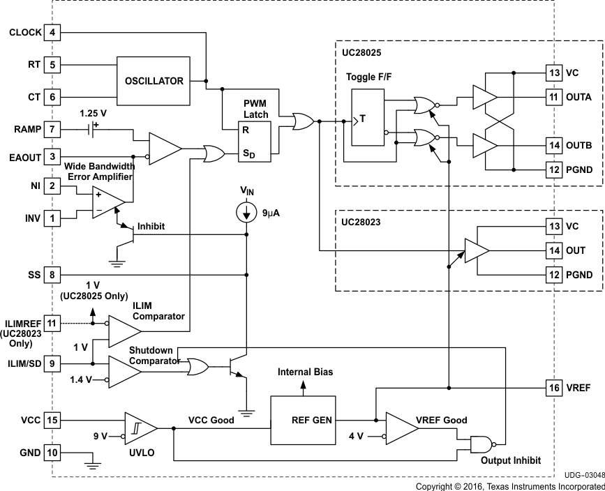
The UC28023 and UC28025 (UC2802x) are fixed-frequency PWM controllers optimized for high-frequency switched-mode power-supply applications. Targeted for cost-effective solutions with minimal external components. UC2802x devices include an oscillator, a temperature-compensated reference, a wide band width error amplifier, a high-speed current-sense comparator, and high-current active-high totem-pole outputs to directly drive external MOSFETs.
Protection circuitry includes a current limit comparator with a 1-V threshold, a TTL compatible shutdown port, and a soft-start pin which doubles as a maximum duty cycle clamp. The logic is fully latched to provide jitter free operation and prohibit multiple pulses at an output. An undervoltage lockout section with 800 mV of hysteresis assures low start-up current. During undervoltage lockout, the outputs are high impedance. Propagation delays through the comparators and logic circuitry have been minimized while maximizing bandwidth and slew rate of the error amplifier.
8.2 Functional Block Diagram
8.3 Feature Description
8.3.1 Error Amplifier
Figure 11 shows a simplified schematic of the UC2802x error amplifier and Figure 2 and Figure 3 show its characteristics.
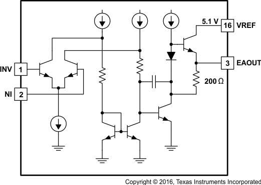 Figure 11. Simplified Error Amplifier Schematic
8.3.2 Synchronization
Figure 12 shows a generalized synchronization. Figure 13 shows a synchronized operation of two units in close proximity.
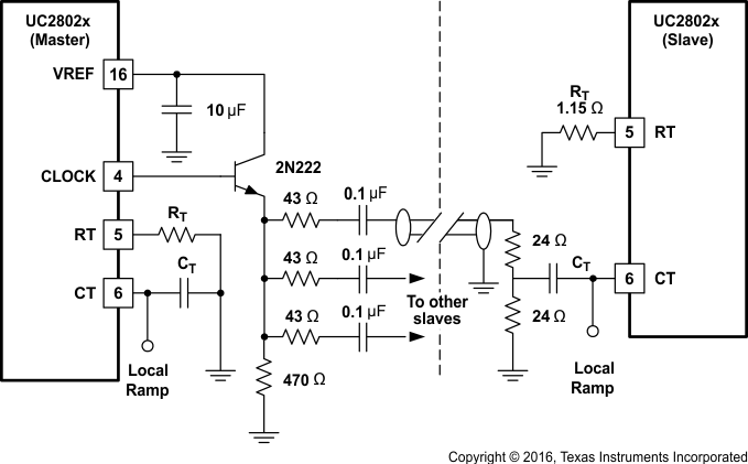 Figure 12. Generalized Synchronization
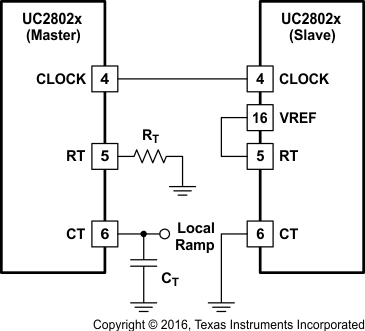 Figure 13. Synchronization of Two Units in Close Proximity
8.3.3 Constant Volt-Second Clamp Circuit
The circuit for the UC28023 shown in Figure 14 describes achievement a constant volt-second product clamp over varying input voltages. The ramp generator components, RT and CR are chosen so that the ramp at Pin 9 (ILIM/SD) crosses the 1-V threshold at the same time the desired maximum volt-second product is reached. The delay through the functional inverter block must be such that the ramp capacitor can be completely discharged during the minimum deadtime.
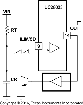 Figure 14. Achieving Constant Volt-Second Product Clamp With the UC28023
The circuit for the UC28025 shown in Figure 15 describes achievement a constant volt-second product clamp over varying input voltages. The ramp generator components, RT and CR are chosen so that the ramp at Pin 9 (ILIM/SD) crosses the 1-V threshold at the same time the desired maximum volt-second product is reached. The delay through the functional inverter block must be such that the ramp capacitor can be completely discharged during the minimum deadtime.
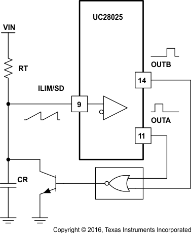 Figure 15. Achieving Constant Volt-Second Product Clamp With the UC28025
8.3.4 Outputs
UC28023 has one output and UC28025 has dual alternating outputs.
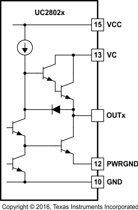 Figure 16. Simplified Schematic
8.3.5 Open-Loop Laboratory Test Fixture
The following test fixture is useful for exercising many of the UC28025’s functions and measuring their specifications. As with any wideband circuit, careful ground and bypass procedures must be followed. TI highly recommends using a ground plane
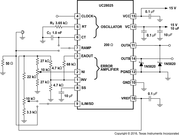 Figure 17. Laboratory Test Fixture
8.4 Device Functional Modes
There are no functional modes for this device.