SLUS224H September 1994 – October 2024 UC1842A , UC1843A , UC1844A , UC1845A , UC2842A , UC2843A , UC2844A , UC2845A , UC3842A , UC3843A , UC3844A , UC3845A
PRODUCTION DATA
- 1
- 1 Features
- 2 Applications
- 3 Description
- 4 Pin Configuration and Functions
- 5 Specifications
- 6 Detailed Description
- 7 Application and Implementation
- 8 Power Supply Recommendations
- 9 Layout
- 10Device and Documentation Support
- 11Revision History
- 12Mechanical, Packaging, and Orderable Information
Package Options
Mechanical Data (Package|Pins)
Thermal pad, mechanical data (Package|Pins)
Orderable Information
7.2.2.2 UC2842A Design Procedure
This application design procedure shows how to setup and use the UC2842A peak current mode controller in an offline flyback converter, with universal input to a 12-V, 48-W regulated output.
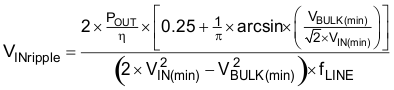
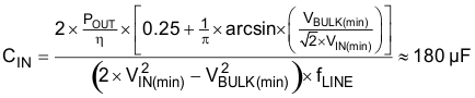
Setting up and designing with the UC2842A peak current mode controller in a continuous mode flyback application requires knowing some things about the power stage. First, calculate the required input bulk capacitance (CIN) based on output power level (POUT), efficiency (ƞ), minimum input voltage (VIN(min)), line frequency (fLINE) and minimum bulk voltage. For this design example let VBULK(min) = 95 V.
The output capacitor (COUT) is sized so the output voltage does not droop more than 10% during a large-signal transient response. The voltage-loop crossover frequency (fC) is estimated to be 2.5 kHz at this point in the design.

The COUT selected for the design is a 2200-µF capacitor, with an equivalent series resistance (ESR) of 45 mΩ.
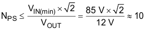
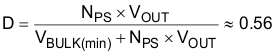
Next calculate the maximum primary to secondary turns ratio (NPS) of the transformer, based on the minimum input voltage and output voltage.
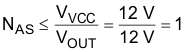
Next calculate the auxiliary to secondary turns ratio (NAS) of the transformer, based on the output voltage and the bias voltage of the UC2842A.
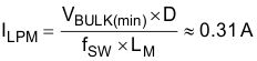
Once the transformer turns ratios have been determined, the minimum primary magnetizing inductance (LPM) of the transformer can be calculated based on minimum bulk voltage, Duty Cycle (D), reflected output current and efficiency. The transformer used in this design has an LPM of 1.7 mH, NPS = 10, and a NAS = 1, fsw = 100 kHz

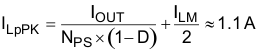
After the transformer has been selected, the primary peak current (ILpPK) of the transformer can be calculated based on the primary magnetizing inductance ripple (ILPM) and the reflected output current across the transformer.
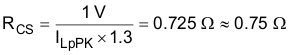
Once the primary peak current has been calculated the current sense resistor (RCS) can be selected.
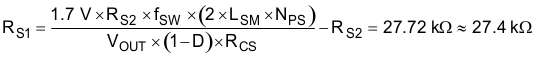
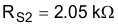
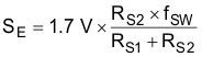
Resistors RS1 and RS2 are used to set the slope compensation of the design. Capacitor CS1 is a DC blocking capacitor, and pull-up resistor RP is used to provide some offset to the current sense signal for noise immunity. RP and RS2 were preselected to add a DC offset of 50 mV to the current sense signal.
RS1 is selected to set the slope compensation to one-half of the ripple current down slope of the flyback inductor. This can be accomplished by calculating the secondary magnetizing inductance (LSM) and using the following calculation for RS1. The 1.7 V in the RS1 equation is the peak-to-peak ripple voltage amplitude of the oscillator.
where
Resistors RI and RK are selected to the output reference and can be calculated by preselecting a value for RK and knowing the TL431 reference voltage (VTL431REF). After choosing 2.49 kΩ for RK, RI is calculated and a standard resistor value of 9.53 kΩ is chosen for this resistor.

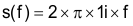
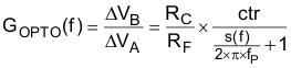
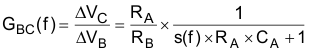
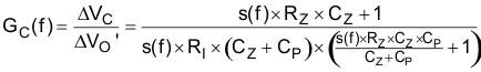
This design using the UC2842A controller has an interesting control loop with many components. GOPTO(f) is the approximate transfer function across the opto isolator in the design. The pole frequency of the opto isolator is represented by fP. The opto isolator used in this design has a current transfer ratio of 1 and pole frequency of roughly 5 kHz. See Figure 7-1 for component placement and node voltages. The voltage loop (fC) must cross-over less than the opto isolator pole for simplified compensation.

GBC(f) is an estimate of the transfer function from the output of the opto isolator to the PWM’s control voltage .
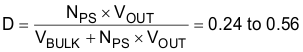
The duty cycle varies with the bulk input voltage (VBULK). VBULK varies from 95 V to 375 V during normal operation. This causes the duty cycle to vary from 24% to 56%.
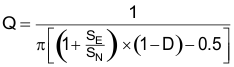
GCO(f) is an estimate of the control (VC) to output transfer function, where variable Q is the quality factor.
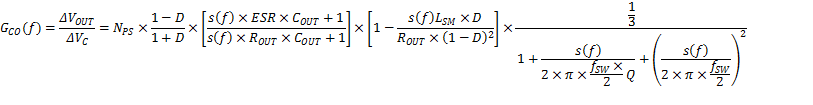
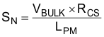
The quality factor (Q) is defined by the primary magnetizing inductance change in voltage (SN) as a function of duty cycle; as well as, the added slope compensation (SE).
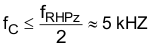
To verify that the voltage loop is stable, the crossover frequency must be less than one half of the right-half-plane zero frequency (fRHPZ) of the flyback converter. The right-half-plane zero frequency at the minimum bulk voltage is approximately 9.8 kHz. For this design example the target crossover of the voltage loop is at 1 kHz. The actual fC can be higher or lower than the target.

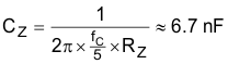
The DC gain of GCO(f) moves with the bulk input voltage. Resistor RZ is selected to crossover the voltage loop when input to the converter is at VBULK(min) and to crossover at 1/5th the maximum crossover frequency.

Capacitor CZ is selected to add 45° of phase margin at voltage loop crossover. For this design example a 6.8-nF capacitor is used.
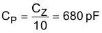
Capacitor CP is selected to attenuate the high frequency gain of the control loop.
GC(f) is the estimated transfer function of the TL431 compensation.
TV(f) is the estimated theoretical transfer function of the close-loop gain of the system. The feedback loop response can be different in the actual circuit and can have to be adjusted with a network analyzer to meet actual circuit performance and reliability. The feedback loop response must be evaluated over worse case variations in design parameters.

For this application example, this design technique generated a theoretical feedback loop (TV(f)) crossover at 1 kHz with roughly 55° of phase margin at a minimum input bulk voltage of 95 V. The theoretical voltage loop at high-line crossed over at 2.7 kHz with a phase margin of 72°. See Figure 7-2 and Figure 7-3. TV(f) must be evaluated with a network analyzer and adjust the loop compensation as necessary based on the actual circuitry behavior. Also conduct transient testing to verify that the device remains stable.