SLUS223H April 1997 – October 2024 UC1842 , UC1843 , UC1844 , UC1845 , UC2842 , UC2843 , UC2844 , UC2845 , UC3842 , UC3843 , UC3844 , UC3845
PRODUCTION DATA
- 1
- 1 Features
- 2 Applications
- 3 Description
- 4 Device Comparison Table
- 5 Pin Configuration and Functions
- 6 Specifications
-
7 Detailed Description
- 7.1 Overview
- 7.2 Functional Block Diagrams
- 7.3 Feature Description
- 7.4 Device Functional Modes
-
8 Application and Implementation
- 8.1 Application Information
- 8.2
Typical Application
- 8.2.1 Design Requirements
- 8.2.2
Detailed Design Procedure
- 8.2.2.1 Input Bulk Capacitor and Minimum Bulk Voltage
- 8.2.2.2 Transformer Turns Ratio and Maximum Duty Cycle
- 8.2.2.3 Transformer Inductance and Peak Currents
- 8.2.2.4 Output Capacitor
- 8.2.2.5 Current Sensing Network
- 8.2.2.6 Gate Drive Resistor
- 8.2.2.7 VREF Capacitor
- 8.2.2.8 RT/CT
- 8.2.2.9 Start-Up Circuit
- 8.2.2.10 Voltage Feedback Compensation
- 8.2.3 Application Curves
- 8.3 Power Supply Recommendations
- 8.4 Layout
- 9 Device and Documentation Support
- 10Revision History
- 11Mechanical, Packaging, and Orderable Information
Package Options
Mechanical Data (Package|Pins)
Thermal pad, mechanical data (Package|Pins)
Orderable Information
5 Pin Configuration and Functions
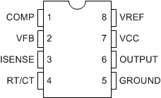
 Figure 5-1 D, JG, and P Packages8-Pin SOIC, CDIP, and PDIPTop View
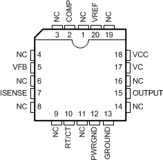
 Figure 5-3 FK Package20-Pin LCCCTop View
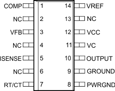
 Figure 5-2 D and W Packages14-Pin SOIC and CFPTop View
| PIN | TYPE(1) | DESCRIPTION | |||
|---|---|---|---|---|---|
| NAME | SOIC, CDIP,
PDIP (8) |
SOIC, CFP (14) |
LCCC (20) |
||
| COMP | 1 | 1 | 2 | O | Error amplifier compensation pin. Connect external compensation components to this pin to modify the error amplifier output. The error amplifier is internally current-limited so the user can command zero duty cycle by externally forcing COMP to GROUND. |
| GROUND | 5 | 9 | 13 | G | Analog ground. For device packages without PWRGND, GROUND functions as both power ground and analog ground. |
| PWRGND | — | 8 | 12 | G | Power ground. For device packages without PWRGND, GROUND functions as both power ground and analog ground |
| ISENSE | 3 | 5 | 7 | I | Primary-side current sense pin. Connect to current sensing resistor. The PWM uses this signal to terminate the OUTPUT switch conduction. A voltage ramp can be applied to this pin to run the device with a voltage-mode control configuration. |
| NC | — | 2, 4, 6, 13 | 1, 3, 4, 6, 8, 9, 11, 14, 16, 19 | — | Do not connect |
| OUTPUT | 6 | 10 | 15 | O | OUTPUT is the gate drive for the external MOSFET. OUTPUT is the output of the on-chip driver stage intended to directly drive a MOSFET. Peak currents of up to 1 A are sourced and sunk by this pin. OUTPUT is actively held low when VCC is below the turnon threshold. |
| RT/CT | 4 | 7 | 10 | I/O | Fixed frequency oscillator set point. Connect timing resistor,
RRT, to VREF and timing capacitor, CCT, to
GROUND from this pin to set the switching frequency. For best
performance, keep the timing capacitor lead to the device GROUND as
short and direct as possible. If possible, use separate ground
traces for the timing capacitor and all other functions. The frequency of the oscillator can be estimated with the following equations: Equation 1.  where fOSC is in Hertz, RRT is in Ohms and CCT is in Farads. Never use a timing resistor less than 5 kΩ. The frequency of the OUTPUT gate drive of the UCx842 and UCx843, fSW, is equal to fOSC at up to 100% duty cycle; the frequency of the UCx844 and UCx845 is equal to half of the fOSC frequency at up to 50% duty cycle. |
| VC | — | 11 | 17 | I | Bias supply input for the output gate drive. For PWM controllers that do not have this pin, the gate driver is biased from the VCC pin. VC must have a bypass capacitor at least 10 times greater than the gate capacitance of the main switching FET used in the design. |
| VCC | 7 | 12 | 18 | I | Analog controller bias input that provides power to the device.
Total VCC current is the sum of the quiescent VCC current and the
average OUTPUT current. Knowing the switching frequency and the
MOSFET gate charge, Qg, the average OUTPUT current can be
calculated from: Equation 2.  A bypass capacitor, typically 0.1 µF, connected directly to GROUND with minimal trace length, is required on this pin. An additional bypass capacitor at least 10 times greater than the gate capacitance of the main switching FET used in the design is also required on VCC. |
| VFB | 2 | 3 | 5 | I | Inverting input to the internal error amplifier. VFB is used to control the power converter voltage-feedback loop for stability. |
| VREF | 8 | 14 | 20 | O | 5-V reference voltage. VREF is used to provide charging current to the oscillator timing capacitor through the timing resistor. Bypassing VREF to GROUND with a ceramic capacitor connected as close to the pin as possible is important for reference stability. A minimum value of 0.1-µF ceramic is required. Additional VREF bypassing is required for external loads on VREF. |