SGLS318A November 2005 – November 2015 UC2854B-EP
PRODUCTION DATA.
- 1 Features
- 2 Applications
- 3 Description
- 4 Revision History
- 5 Description (continued)
- 6 Pin Configuration and Functions
- 7 Specifications
- 8 Detailed Description
-
9 Application and Implementation
- 9.1 Application Information
- 9.2
Typical Application
- 9.2.1 Design Requirements
- 9.2.2
Detailed Design Procedure
- 9.2.2.1 Switching Frequency
- 9.2.2.2 Inductor Selection
- 9.2.2.3 Output Capacitor
- 9.2.2.4 Switch and Diode
- 9.2.2.5 Current Sensing
- 9.2.2.6 Peak Current Limit
- 9.2.2.7 Multiplier Set-up
- 9.2.2.8 Feedforward Voltage
- 9.2.2.9 Multiplier Input Current
- 9.2.2.10 Oscillator Frequency
- 9.2.2.11 Current Error Amplifier Compensation
- 9.2.2.12 Voltage Error Amplifier Compensation
- 9.2.2.13 Feedforward Voltage Divider Filter Capacitors
- 9.2.2.14 Design Procedure Summary
- 9.2.3 Application Curve
- 10Power Supply Recommendations
- 11Layout
- 12Device and Documentation Support
- 13Mechanical, Packaging, and Orderable Information
Package Options
Mechanical Data (Package|Pins)
- DW|16
Thermal pad, mechanical data (Package|Pins)
- DW|16
Orderable Information
7 Specifications
7.1 Absolute Maximum Ratings
over operating free-air temperature range (unless otherwise noted)(1)| MIN | MAX | UNIT | ||
|---|---|---|---|---|
| VCC | Supply voltage | 22 | V | |
| Input voltage | VSENSE, VRMS, ISENSE MOUT | 11 | V | |
| PKLMT | 5 | V | ||
| IGTDRV | GTDRV current, continuous | 0.5 | A | |
| IGTDRV | GTDRV current, 50% duty cycle | 1.5 | A | |
| Input current | RSET, IAC, PKLMT, ENA | 10 | mA | |
| TJ | Junction temperature | −55 | 150 | °C |
| Tsol | Lead temperature, 1.6 mm (1/16 inch) from case for 10 seconds | 300 | °C | |
| Tstg | Storage temperature | −65 | 150 | °C |
(1) Stresses beyond those listed under Absolute Maximum Ratings may cause permanent damage to the device. These are stress ratings only, which do not imply functional operation of the device at these or any other conditions beyond those indicated under Recommended Operating Conditions. Exposure to absolute-maximum-rated conditions for extended periods may affect device reliability.
7.2 ESD Ratings
| VALUE | UNIT | |||
|---|---|---|---|---|
| V(ESD) | Electrostatic discharge | Human-body model (HBM), per ANSI/ESDA/JEDEC JS-001(1) | ±2000 | V |
(1) JEDEC document JEP155 states that 500-V HBM allows safe manufacturing with a standard ESD control process.
7.3 Recommended Operating Conditions
over operating free-air temperature range (unless otherwise noted)| MIN | MAX | UNIT | ||
|---|---|---|---|---|
| VCC | Supply voltage | 10 | 20 | V |
| TJ | Operating junction temperature | −55 | 125 | °C |
7.4 Thermal Information
| THERMAL METRIC(1) | UC2854B-EP | UNIT | ||
|---|---|---|---|---|
| DW (SOIC) | ||||
| 16 PINS | ||||
| HIGH | LOW | |||
| RθJA | Junction-to-ambient thermal resistance (2) | 36.9 | 38.4 | °C/W |
| RθJC | Junction-to-case thermal resistance | 73.1 | 111.6 | °C/W |
(1) For more information about traditional and new thermal metrics, see the Semiconductor and IC Package Thermal Metrics application report, SPRA953.
(2) RθJA values are based on zero air flow.
7.5 Electrical Characteristics
over operating free-air temperature range (unless otherwise noted)| PARAMETER | TEST CONDITIONS | MIN | TYP | MAX | UNIT | |
|---|---|---|---|---|---|---|
| OVERALL | ||||||
| Supply current, off | CAO = 0 V, VAO = 0 V, VCC = VUVLO − 0.3 V | 250 | 400 | µA | ||
| Supply current, on | 12 | 18 | mA | |||
| VCC turn-on threshold voltage | 8 | 10.5 | 11.3 | V | ||
| VCC turn-off threshold voltage | 9 | 10 | 12 | V | ||
| VCC clamp | IVCC = IVCC(on) + 5 mA | 18 | 20 | 22 | V | |
| VOLTAGE AMPLIFIER | ||||||
| Input voltage | 2.9 | 3 | 3.1 | V | ||
| VSENSE bias current | −500 | −25 | 500 | nA | ||
| Open loop gain | 2 V ≤ VOUT ≤ 5 V | 70 | 100 | dB | ||
| VOH | High-level output voltage | ILOAD = −500 µA | 6 | V | ||
| VOL | Low-level output voltage | ILOAD = 500 µA | 0.3 | 0.5 | V | |
| ISC | Output short-circuit current | VOUT = 0 V | 1.5 | 3.5 | mA | |
| Gain bandwidth product(1) | fIN = 100 kHz, 10 mVP−P | 1 | MHz | |||
| CURRENT AMPLIFIER | ||||||
| Input offset voltage | VCM = 0 V, TA = 25°C | −4 | 0 | mV | ||
| VCM = 0 V, overtemperature | −5.5 | 0 | ||||
| Input bias current, ISENSE | VCM = 0 V | −500 | 500 | nA | ||
| Open loop gain | 2 V ≤ VOUT ≤ 6 V | 80 | 110 | dB | ||
| VOH | High-level output voltage | ILOAD = −500 µA | 8 | V | ||
| VOL | Low-level output voltage | ILOAD = 500 µA | 0.3 | 0.5 | V | |
| ISC Output short-circuit current | VOUT = 0 V | 1.5 | 3.5 | mA | ||
| CMRR Common mode rejection range | −0.3 | 5 | V | |||
| Gain bandwidth product(1) | fIN = 100 kHz, 10 mVP−P | 3 | 5 | MHz | ||
| REFERENCE | ||||||
| Output voltage | IREF = 0 mA, TA = 25°C | 7.4 | 7.5 | 7.6 | V | |
| IREF = 0 mA | 7.35 | 7.5 | 7.65 | |||
| Load regulation | 1 mA ≤ IREF ≤ 10 mA | 0 | 8 | 20 | mV | |
| Line regulation | 12 V ≤ VCC ≤ 18 V | 0 | 14 | 25 | mV | |
| ISC Short circuit current | VREF = 0 V | 25 | 35 | 60 | mA | |
| OSCILLATOR | ||||||
| Initial accuracy | TA = 25°C | 85 | 100 | 115 | kHz | |
| Voltage stability | 12 V ≤ VCC ≤ 18 V | 1% | ||||
| Total variation | Line, temperature | 80 | 120 | kHz | ||
| Ramp amplitude (peak-to-peak) | 4.9 | 5.9 | ||||
| Ramp valley voltage | 0.8 | 1.3 | V | |||
| ENABLE/SOFT-START/CURRENT LIMIT | ||||||
| Enable threshold voltage | 2.35 | 2.55 | 2.90 | V | ||
| Enable hysteresis | VFAULT = 2.5 V | 500 | 600 | mV | ||
| Enable input bias current | VENA = 0 V | −2 | −5 | µA | ||
| Propagation delay to disable time(1) | Enable overdrive = 100 mV | 300 | ns | |||
| Soft-start charge current | VSS = 2.5 V | 10 | 14 | 24 | µA | |
| Peak limit offset voltage | −15 | 15 | mV | |||
| Peak limit input current | VPKLMT = −0.1 V | −200 | −100 | µA | ||
| Peak limit propagation delay time(1) | 150 | ns | ||||
| MULTIPLIER | ||||||
| Output current, IAC limited | IAC = 100 µA, VRMS = 1 V, RSET = 10 kΩ | −220 | −200 | −170 | µA | |
| Output current, zero | IAC = 0 µA, RSET = 10 kΩ | −2 | −0.2 | 2 | µA | |
| Output current, power limited | VRMS = 1.5 V, VA = 6 V | −230 | −200 | −170 | µA | |
| Output current | VRMS = 1.5 V, VA = 2 V | −22 | µA | |||
| VRMS = 1.5 V, VA = 5 V | −156 | |||||
| VRMS = 5 V, VA = 2 V | −2 | |||||
| VRMS = 5 V, VA = 5 V | −14 | |||||
| Gain constant(2) | VRMS = 1.5 V, VA = 6 V, TA = 25°C | −1.1 | −1 | −0.9 | A/A | |
| GATE DRIVER | ||||||
| VOH | High-level output voltage | IOUT = −200 mA, VCC = 15 V | 12 | 12.8 | V | |
| VOL | Low-level output voltage | IOUT = 200 mA | 1 | 2.2 | V | |
| IOUT = 10 mA | 300 | 500 | mV | |||
| Low-level UVLO voltage | IOUT = 50 mA, VCC = 0 V | 0.9 | 1.5 | V | ||
| Output rise time(1) | CLOAD = 1 nF | 35 | ns | |||
| Output fall time(1) | CLOAD = 1 nF | 35 | ns | |||
| Output peak current(1) | CLOAD = 10 nF | 1 | A | |||
(1) Ensured by design. Not production tested.
(2) Gain constant. 

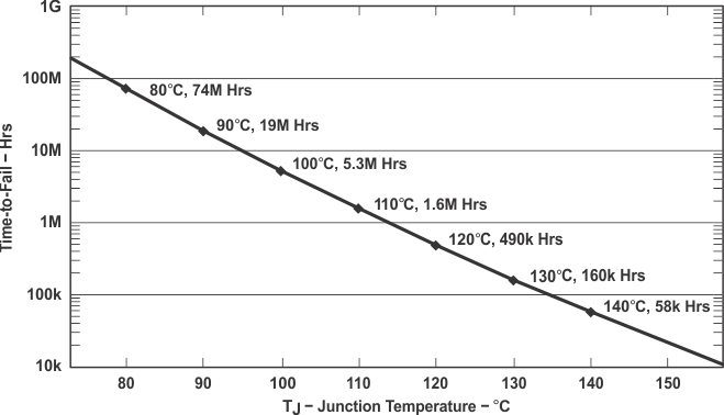
 Figure 1. Wirebond Operating Life Derating Chart
7.6 Typical Characteristics


