SLUS224H September   1994  – October 2024 UC1842A , UC1843A , UC1844A , UC1845A , UC2842A , UC2843A , UC2844A , UC2845A , UC3842A , UC3843A , UC3844A , UC3845A

PRODUCTION DATA  

  1.   1
  2. Features
  3. Applications
  4. Description
  5. Pin Configuration and Functions
  6. Specifications
    1. 5.1 Absolute Maximum Ratings
    2. 5.2 ESD Ratings
    3. 5.3 Recommended Operating Conditions
    4. 5.4 Thermal Information
    5. 5.5 Electrical Characteristics
    6. 5.6 Typical Characteristics
  7. Detailed Description
    1. 6.1 Overview
    2. 6.2 Functional Block Diagram
    3. 6.3 Feature Description
      1. 6.3.1 Pulse-by-Pulse Current Limiting
      2. 6.3.2 Current Sense Circuit
      3. 6.3.3 Error Amplifier Configuration
      4. 6.3.4 Undervoltage Lockout
      5. 6.3.5 Oscillator
    4. 6.4 Device Functional Modes
      1. 6.4.1 Normal Operation
      2. 6.4.2 Undervoltage Lockout (UVLO) Start-Up
      3. 6.4.3 UVLO Turnoff Mode
  8. Application and Implementation
    1. 7.1 Application Information
    2. 7.2 Typical Application
      1. 7.2.1 Design Requirements
      2. 7.2.2 Detailed Design Procedure
        1. 7.2.2.1 Custom Design With WEBENCH® Tools
        2. 7.2.2.2 UC2842A Design Procedure
      3. 7.2.3 Application Curves
  9. Power Supply Recommendations
  10. Layout
    1. 9.1 Layout Guidelines
    2. 9.2 Layout Example
  11. 10Device and Documentation Support
    1. 10.1 Device Support
      1. 10.1.1 Development Support
        1. 10.1.1.1 Custom Design With WEBENCH® Tools
      2. 10.1.2 Device Nomenclature
    2. 10.2 Documentation Support
      1. 10.2.1 Related Documentation
    3. 10.3 Related Links
    4. 10.4 Receiving Notification of Documentation Updates
    5. 10.5 Support Resources
    6. 10.6 Trademarks
    7. 10.7 Electrostatic Discharge Caution
    8. 10.8 Glossary
  12. 11Revision History
  13. 12Mechanical, Packaging, and Orderable Information

Package Options

Mechanical Data (Package|Pins)
Thermal pad, mechanical data (Package|Pins)
Orderable Information

Oscillator

UC1842A UC1843A UC1844A UC1845A  UC2842A UC2843A UC2844A UC2845A  UC3842A UC3843A UC3844A UC3845A Oscillator Frequency vs Timing ResistanceFigure 6-4 Oscillator Frequency vs Timing Resistance
UC1842A UC1843A UC1844A UC1845A  UC2842A UC2843A UC2844A UC2845A  UC3842A UC3843A UC3844A UC3845A Maximum Duty Cycle vs Timing ResistanceFigure 6-5 Maximum Duty Cycle vs Timing Resistance
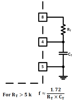
UC1842A UC1843A UC1844A UC1845A  UC2842A UC2843A UC2844A UC2845A  UC3842A UC3843A UC3844A UC3845A Oscillator SectionFigure 6-6 Oscillator Section
UC1842A UC1843A UC1844A UC1845A  UC2842A UC2843A UC2844A UC2845A  UC3842A UC3843A UC3844A UC3845A Slope CompensationFigure 6-7 Slope Compensation

Precision operation at high frequencies with an accurate maximum duty cycle, see Figure 6-5, can be obtained with the UCx84xA family of devices due to the trimmed oscillator discharge current. This nullifies the effects of production variations in the initial discharge current or dead time. Previous versions of the UCx84x devices had greater than a 2:1 oscillator discharge current range and resulted in less reliable maximum duty cycle programming.

A fraction of the oscillator ramp can be resistively summed with the current sense signal, to provide slope compensation for converters requiring duty cycles over 50%. Capacitor C forms a filter with R2 to suppress the leading-edge switch spikes.