SLUS223H April 1997 – October 2024 UC1842 , UC1843 , UC1844 , UC1845 , UC2842 , UC2843 , UC2844 , UC2845 , UC3842 , UC3843 , UC3844 , UC3845
PRODUCTION DATA
- 1
- 1 Features
- 2 Applications
- 3 Description
- 4 Device Comparison Table
- 5 Pin Configuration and Functions
- 6 Specifications
-
7 Detailed Description
- 7.1 Overview
- 7.2 Functional Block Diagrams
- 7.3 Feature Description
- 7.4 Device Functional Modes
-
8 Application and Implementation
- 8.1 Application Information
- 8.2
Typical Application
- 8.2.1 Design Requirements
- 8.2.2
Detailed Design Procedure
- 8.2.2.1 Input Bulk Capacitor and Minimum Bulk Voltage
- 8.2.2.2 Transformer Turns Ratio and Maximum Duty Cycle
- 8.2.2.3 Transformer Inductance and Peak Currents
- 8.2.2.4 Output Capacitor
- 8.2.2.5 Current Sensing Network
- 8.2.2.6 Gate Drive Resistor
- 8.2.2.7 VREF Capacitor
- 8.2.2.8 RT/CT
- 8.2.2.9 Start-Up Circuit
- 8.2.2.10 Voltage Feedback Compensation
- 8.2.3 Application Curves
- 8.3 Power Supply Recommendations
- 8.4 Layout
- 9 Device and Documentation Support
- 10Revision History
- 11Mechanical, Packaging, and Orderable Information
Package Options
Mechanical Data (Package|Pins)
Thermal pad, mechanical data (Package|Pins)
Orderable Information
8.2.2.3 Transformer Inductance and Peak Currents
For this design example, the transformer magnetizing inductance is selected based upon the CCM condition. An inductance value that allows the converter to stay in CCM over a wider operating range before transitioning into discontinuous current mode is used to minimize losses due to otherwise high currents and also to decrease the output ripple. The design of the transformer in this example sizes the inductance so the converter enters CCM operation at approximately 10% load and minimum bulk voltage to minimize output ripple.
The inductor, LP for a CCM flyback can be calculated using Equation 17.

In Equation 17, the input power, PIN, is estimated by dividing the maximum output power, POUT, by the target efficiency, η, and fSW is the switching frequency; for the UC2842 the switching frequency is equal to the oscillator frequency and is set to 110 kHz. Therefore, the transformer inductance can be approximately 1.8 mH; a 1.5-mH inductance is chosen as the magnetizing inductance value for this design.
Based on calculated inductor value and the switching frequency, the current stress of the MOSFET and output diode can be calculated.
The peak current in the primary-side MOSFET of a CCM flyback can be calculated as shown in Equation 18.
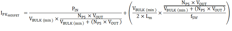
The MOSFET peak current is 1.36 A. The RMS current of the MOSFET is calculated to be 0.97 A as shown in Equation 19. Therefore, IRFB9N65A is selected to be used as the primary-side switch.
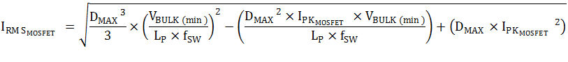
The output diode peak current is equal to the MOSFET peak current reflected to the secondary side.

The diode average current is equal to the total output current, 4 A; combined with a required 60-V rating and 13.6-A peak current requirement, a 48CTQ060-1 is selected for the output diode.