SLUSEV9A August   2023  – September 2023 UCC14340-Q1

PRODUCTION DATA  

  1.   1
  2. Features
  3. Applications
  4. Description
  5. Revision History
  6. Device Comparison
  7. Pin Configuration and Functions
  8. Specifications
    1. 7.1 Absolute Maximum Ratings
    2. 7.2 ESD Ratings
    3. 7.3 Recommended Operating Conditions
    4. 7.4 Thermal Information
    5. 7.5 Insulation Specifications
    6. 7.6 Safety-Related Certifications
    7. 7.7 Electrical Characteristics
    8. 7.8 Safety Limiting Values
    9. 7.9 Typical Characteristics
  9. Detailed Description
    1. 8.1 Overview
    2. 8.2 Functional Block Diagram
    3. 8.3 Feature Description
      1. 8.3.1 Power Stage Operation
        1. 8.3.1.1 VDD-VEE Voltage Regulation
        2. 8.3.1.2 COM-VEE Voltage Regulation
        3. 8.3.1.3 Power Handling Capability
      2. 8.3.2 Output Voltage Soft Start
      3. 8.3.3 ENA and PG
      4. 8.3.4 Protection Functions
        1. 8.3.4.1 Input Undervoltage Lockout
        2. 8.3.4.2 Input Overvoltage Lockout
        3. 8.3.4.3 Output Undervoltage Protection
        4. 8.3.4.4 Output Overvoltage Protection
        5. 8.3.4.5 Overpower Protection
        6. 8.3.4.6 Overtemperature Protection
    4. 8.4 Device Functional Modes
  10. Application and Implementation
    1. 9.1 Application Information
    2. 9.2 Typical Application
      1. 9.2.1 Design Requirements
      2. 9.2.2 Detailed Design Procedure
        1. 9.2.2.1 Capacitor Selection
        2. 9.2.2.2 Single RLIM Resistor Selection
        3. 9.2.2.3 RDR Circuit Component Selection
        4. 9.2.2.4 Feedback Resistors Selection
  11. 10System Examples
  12. 11Power Supply Recommendations
  13. 12Layout
    1. 12.1 Layout Guidelines
    2. 12.2 Layout Example
  14. 13Device and Documentation Support
    1. 13.1 Documentation Support
      1. 13.1.1 Related Documentation
    2. 13.2 Receiving Notification of Documentation Updates
    3. 13.3 Support Resources
    4. 13.4 Trademarks
    5. 13.5 Electrostatic Discharge Caution
    6. 13.6 Glossary
  15. 14Mechanical, Packaging, and Orderable Information
  16. 15Tape and Reel Information

Package Options

Mechanical Data (Package|Pins)
Thermal pad, mechanical data (Package|Pins)
Orderable Information

Description

UCC14340-Q1 is a high isolation voltage DC/DC module designed to provide power to IGBT or SiC gate drivers. The module integrates a transformer and DC/DC controller with a proprietary architecture to achieve high efficiency with very low emissions. The high-accuracy output voltages provide higher system efficiency without over-stressing the power device gate.

The fully integrated module with on-chip device protection requires a minimum of external components, and provides extra features such as input under-voltage lockout, over-voltage lockout, output voltage powergood comparators, over-temperature shutdown, soft-start timing, adjustable isolated positive and negative output voltage, an enable pin, and an open-drain output powergood pin.

Device Information
ORDERABLE PART NUMBER(1)PACKAGEBODY SIZE (NOM)
UCC14340QDWNRQ1SSOP12.83 mm × 7.50 mm
For all available packages, see the orderable addendum at the end of the data sheet.
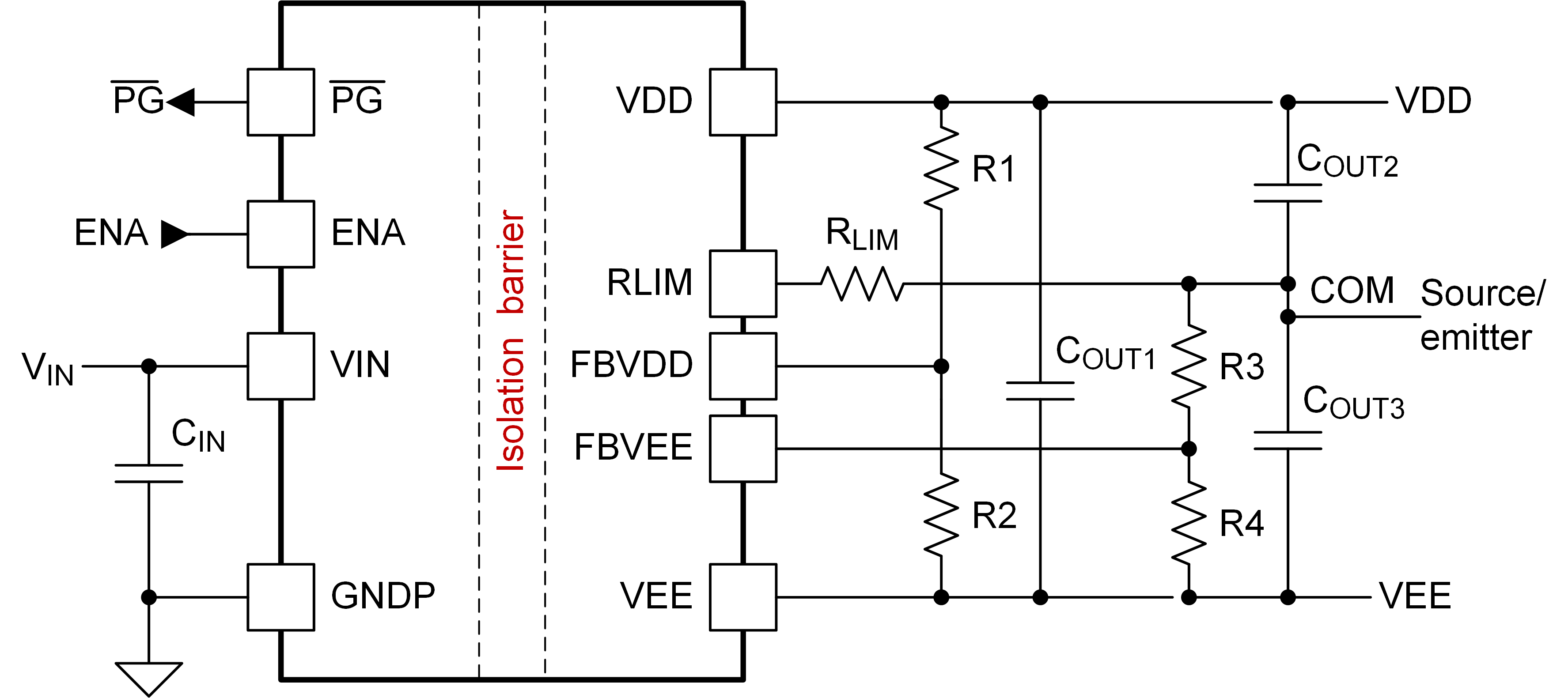
GUID-7AC281E7-3B24-4CEC-8112-C5793A47AEBB-low.gif Simplified Application
GUID-F7A1F42D-F745-4D08-8B12-3E504A4BF2E5-low.svgTypical Power-up Sequence