SLUSEV9A August 2023 – September 2023 UCC14340-Q1
PRODUCTION DATA
- 1
- 1 Features
- 2 Applications
- 3 Description
- 4 Revision History
- 5 Device Comparison
- 6 Pin Configuration and Functions
- 7 Specifications
- 8 Detailed Description
- 9 Application and Implementation
- 10System Examples
- 11Power Supply Recommendations
- 12Layout
- 13Device and Documentation Support
- 14Mechanical, Packaging, and Orderable Information
- 15Tape and Reel Information
Package Options
Mechanical Data (Package|Pins)
- DWN|36
Thermal pad, mechanical data (Package|Pins)
Orderable Information
9.2.2.4 Feedback Resistors Selection
VVDD-VEE Regulation
The VVDD-VEE output voltage is regulated by sensing with a feedback resistor divider, where a resistor from VDD to VEE (RFBVDD_VDD) and a resistor from COM to VEE (RFBVDD_VEE) are used so that FBVDD = 2.5V
Use 0.1% resistors for the highest accuracy. External resistor divider will help to cancel the temperature coefficient of the resistors. We can set resistor RFBVDD_VEE = 10k ohm, then calculate for resistor RFBVDD_VDD using the following equation.
A 330pF ceramic capacitor, CFBVDD, must be connected from FBVDD to VEE to filter high frequency switching noise. This capacitor should be in parallel to the RFBVDD_VEE resistor.
VVCOM-VEE Regulation
Similarly, in dual output applications, the VCOM-VEE voltage can be regulated by sensing the output voltage with a resistor divider; however there are three different feedback resistor configurations depending on whether regulation voltage desired is greater-than 2.5V, or equal-to 2.5V, or less-than 2.5V. For all three configurations, a 330pF ceramic capacitor must be connected from FBVEE to VEE to filter high frequency switching noise.
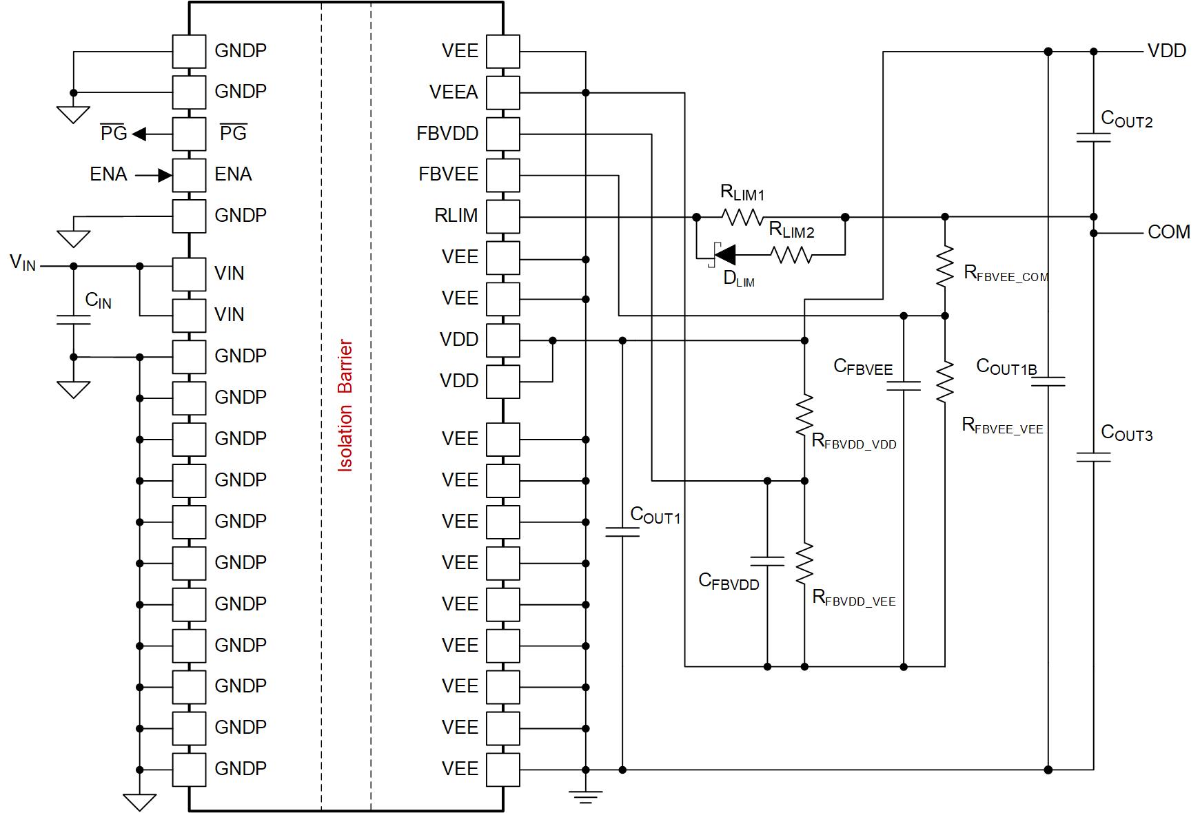
VVCOM-VEE > 2.5V: When the VCOM-VEE regulation voltage is greater-than 2.5V, the resistors RFBVEE_COM and RFBVEE_VEE are connected as shown in figure below (Dual output application schematic configured for VCOM_VEE regulation > 2.5V) between COM and VEE. Letting RFBVEE_COM = 10k ohms, we can calculate RFBVEE_VEE with the following equation.
Connect a 330pF ceramic capacitor, CFBVEE, from FBVEE to VEE for filtering high frequency switching noise.
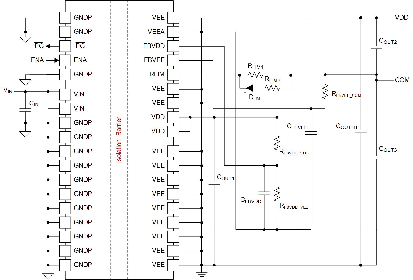
VVCOM-VEE = 2.5V: When the VCOM-VEE regulation voltage is equal-to 2.5V, only a single resistor, RFBVEE_COM is needed connected from COM to FBVEE as shown in figure below (Dual output application schematic configured for VCOM_VEE regulation = 2.5V). Select RFBVEE_COM = 10k ohms. This sets the corner frequency for the high frequency filter with the 330pF capacitor, CFBVEE, connected from FBVEE to VEE.
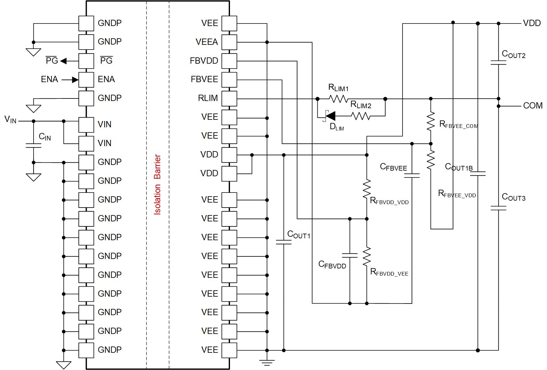
VVCOM-VEE < 2.5V: When the VCOM-VEE regulation voltage is less-than 2.5V, the resistors RFBVEE_COM and RFBVEE_VDD are connected as shown in figure below (Dual output application schematic configured for VCOM_VEE regulation > 2.5V) between VDD and COM. Letting RFBVEE_COM = 10k ohms, we can calculate RFBVEE_VDD with the following equation.
Connect a 330pF ceramic capacitor, CFBVEE, from FBVEE to VEE to filter high frequency switching noise.
 Figure 9-8 Dual output application schematic configured for VCOM_VEE regulation > 2.5V
 Figure 9-9 Dual output application schematic configured for VCOM_VEE regulation = 2.5V
 Figure 9-10 Dual output application schematic configured for VCOM_VEE regulation < 2.5V