SLUSF11C February 2023 – March 2024 UCC14341-Q1
PRODUCTION DATA
- 1
- 1 Features
- 2 Applications
- 3 Description
- 4 Device Comparison
- 5 Pin Configuration and Functions
- 6 Specifications
- 7 Detailed Description
- 8 Application and Implementation
- 9 Device and Documentation Support
- 10Revision History
- 11Mechanical, Packaging, and Orderable Information
- 12Tape and Reel Information
Package Options
Mechanical Data (Package|Pins)
- DWN|36
Thermal pad, mechanical data (Package|Pins)
Orderable Information
6.10 Typical Characteristics
The maximum recommended average power safe
operating area (SOA) at each VIN is determined by the lower value of the 1.5W
limit (dotted line) and the corresponding thermal derating curve (solid line) at that
input voltage. Ambient temperatures higher than 125oC is not recommended. The
thermal derating power is acquired with an evaluation board similar to the EVM shown in
the Layout Example section. Tshut represents the primary-side
over-temperature shutdown rising threshold. As shown in the Electrical Characteristics
table, the typical Tshut value is 160oC, and minimal
Tshut value is 150oC. The SOA derating curve with both
Tshut = 160oC and 150oC are provided below. The SOA
curves under four common VDD-VEE settings, 15V, 18V, 22V, and 25V are characterized. In
each SOA curve, the input voltage is swept from 9V to 18V. To represent a worst-case
condition with Tshut = 150oC, the test is done in a shieded box to
block circulating air in the thermal chamber.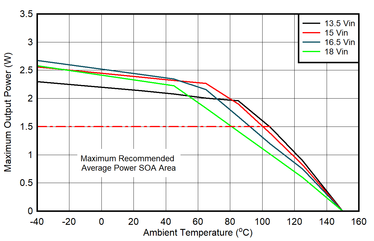 Figure 6-2 SOA
Derating Curves: VVDD-VEE = 15V, VCOM-VEE = 5V,
Tshut=160oC, No Load on
VCOM-VEE
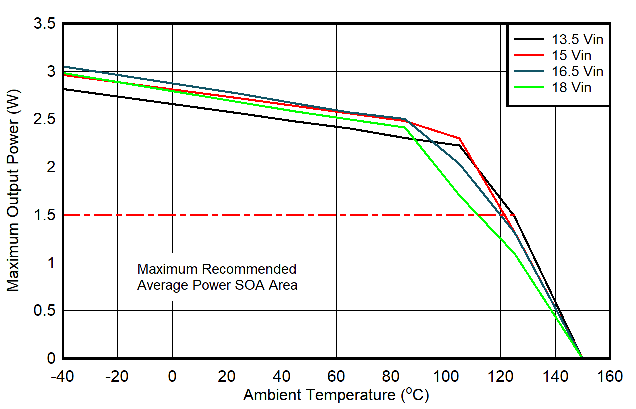 Figure 6-4 SOA
Derating Curves: VVDD-VEE = 22V, VCOM-VEE = 4V,
Tshut=160oC, No Load on
VCOM-VEE
 Figure 6-6 SOA Derating Curves:
VVDD-VEE = 22V, VCOM-VEE = 4V,
Tshut=150oC, No Load on VCOM-VEE,
tested in a shielded box.
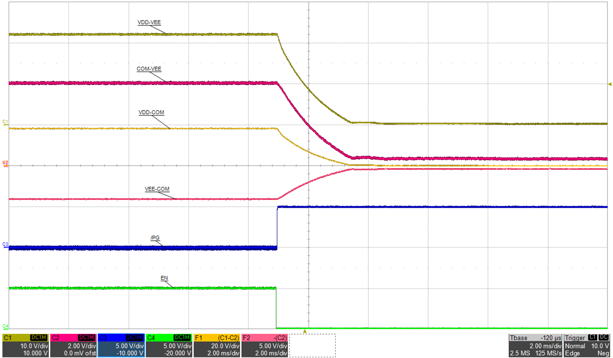 Figure 6-8 Shutdown: VIN = 15V, VVDD-VEE = 22V,
VCOM-VEE = 4V, IVDD-VEE = 68mA, No Load on
VCOM-VEE. Time Scale: 2ms/div.
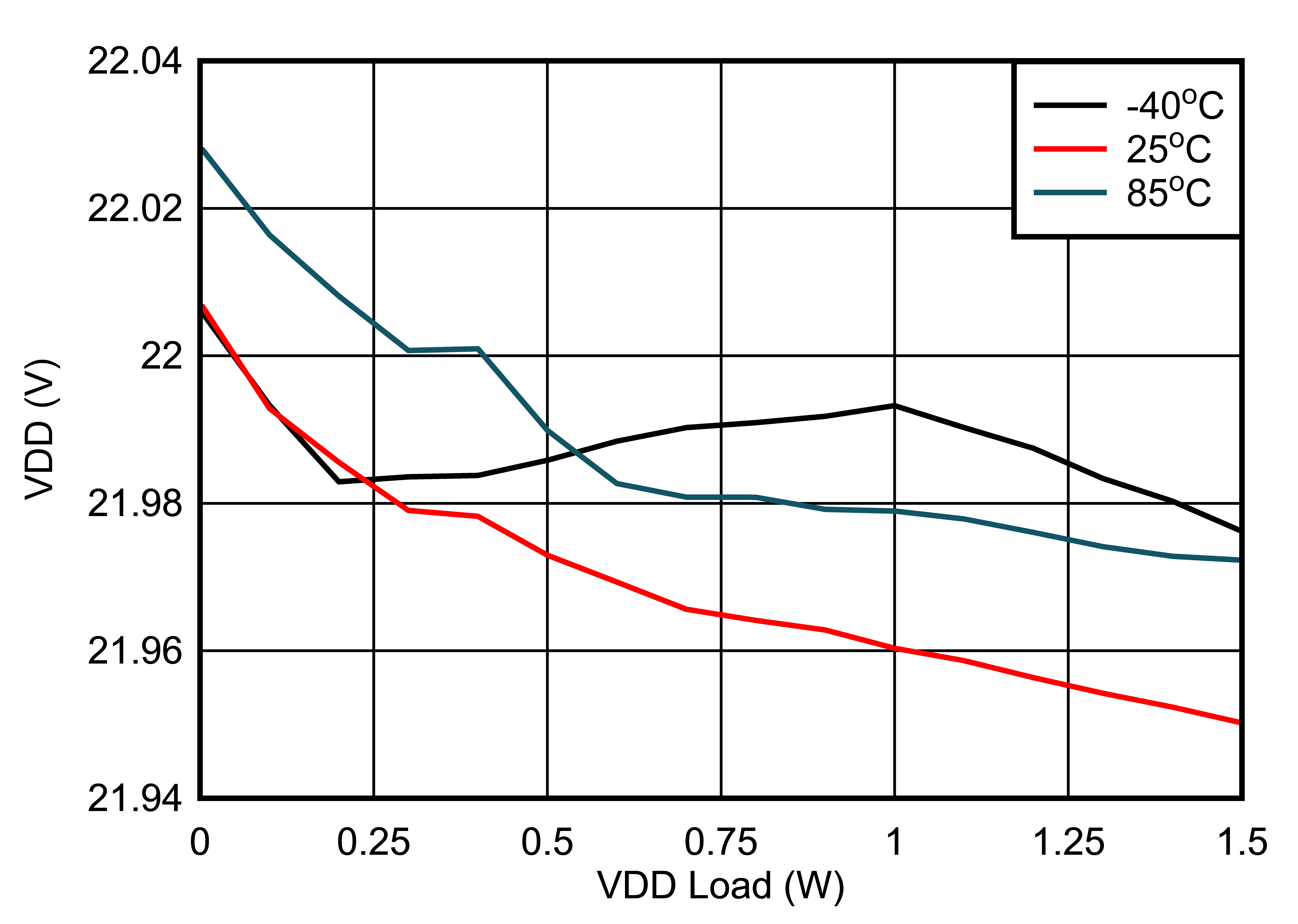 Figure 6-10 VVDD-VEE Load Regulation: VIN = 13.5V,
VVDD-VEE = 22V, VCOM-VEE = 4V
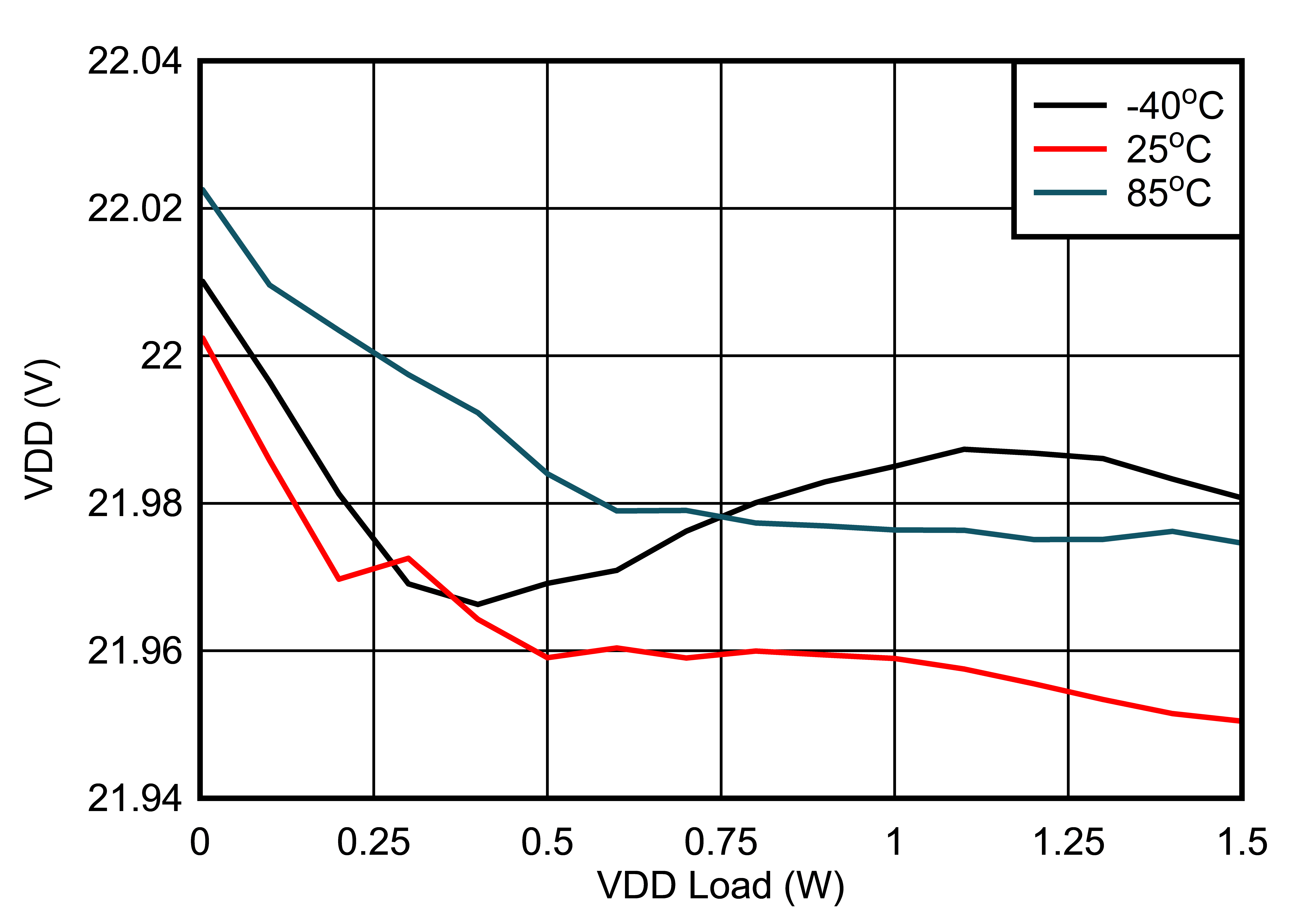 Figure 6-12 VVDD-VEE Load Regulation: VIN = 16.5V,
VVDD-VEE = 22V, VCOM-VEE = 4V
 Figure 6-14 VCOM-VEE Load Regulation: VIN = 13.5V,
VVDD-VEE = 22V, VCOM-VEE = 4V
 Figure 6-16 VCOM-VEE Load Regulation: VIN = 16.5V,
VVDD-VEE = 22V, VCOM-VEE = 4V
 Figure 6-18 Efficiency vs. Load on VVDD-VEE: VIN = 13.5V,
VVDD-VEE = 22V, VCOM-VEE = 4V, No Load on
VCOM-VEE
 Figure 6-20 Efficiency vs. Load on VVDD-VEE: VIN = 16.5V,
VVDD-VEE = 22V, VCOM-VEE = 4V, No Load on
VCOM-VEE
 Figure 6-22 Input
Current vs. Load on VVDD-VEE: VIN = 13.5V,
VVDD-VEE = 22V, VCOM-VEE = 4V, No Load on
VCOM-VEE
 Figure 6-24 Input
Current vs. Load on VVDD-VEE: VIN = 16.5V,
VVDD-VEE = 22V, VCOM-VEE = 4V, No Load on
VCOM-VEE
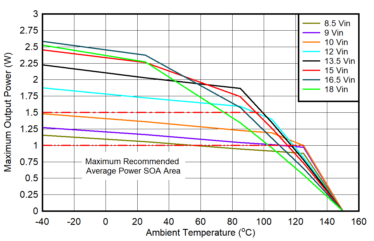 Figure 6-26 UCC14341B-Q1 SOA Derating Curves: VVDD-VEE = 15V,
VCOM-VEE = 5V, Tshut=160oC, No Load on
VCOM-VEE
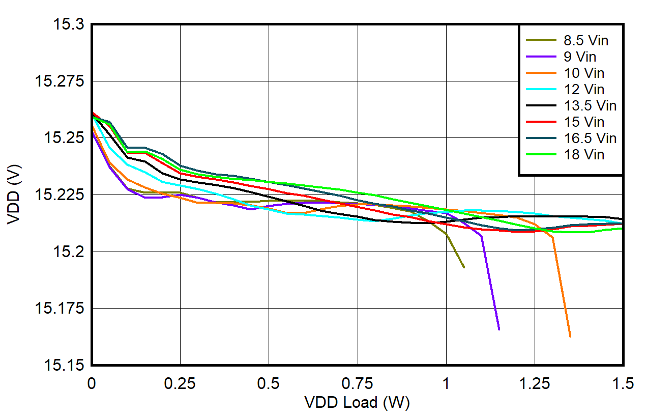 Figure 6-28 UCC14341B-Q1 VVDD-VEE Load Regulation: TAMBIENT =
25oC, VVDD-VEE = 15V, VCOM-VEE =
4V
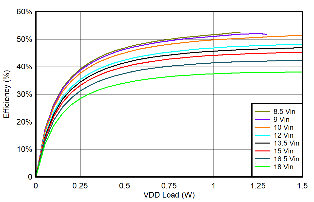 Figure 6-30 UCC14341B-Q1 Efficiency vs. Load on VVDD-VEE:
TAMBIENT = -40oC, VVDD-VEE = 15V,
VCOM-VEE = 4V, No Load on VCOM-VEE
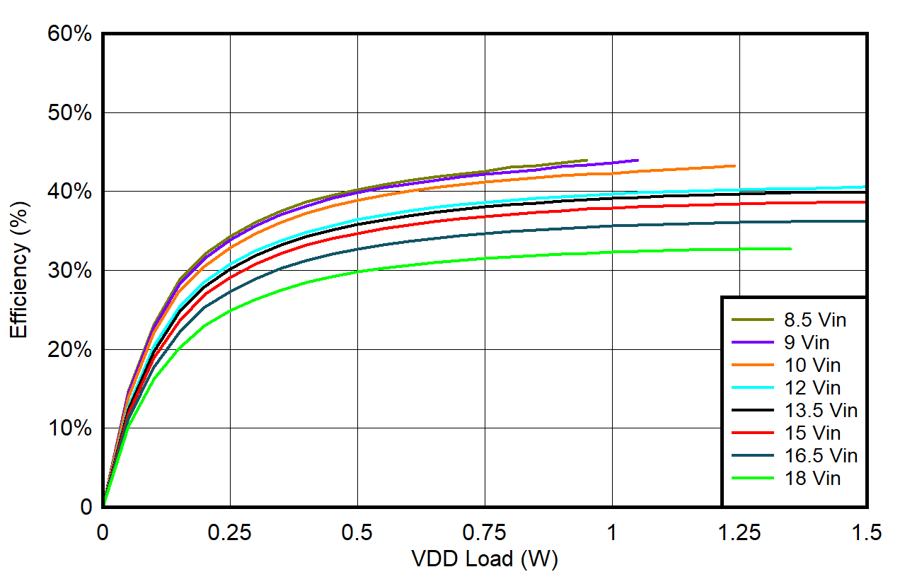 Figure 6-32 UCC14341B-Q1 Efficiency vs. Load on VVDD-VEE:
TAMBIENT = 85oC, VVDD-VEE = 15V,
VCOM-VEE = 4V, No Load on VCOM-VEE
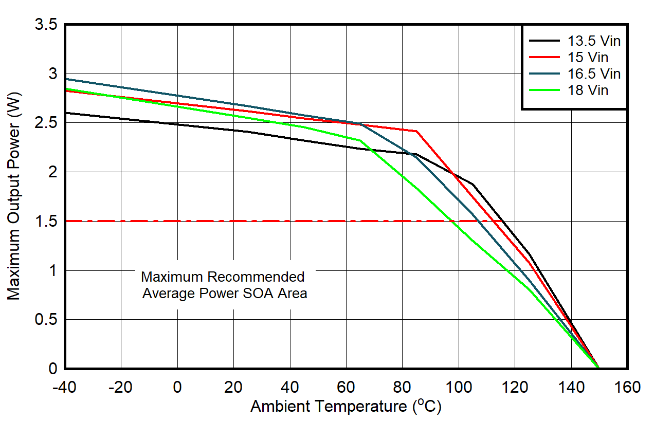 Figure 6-3 SOA
Derating Curves: VVDD-VEE = 18V, VCOM-VEE = 3V,
Tshut=160oC, No Load on
VCOM-VEE
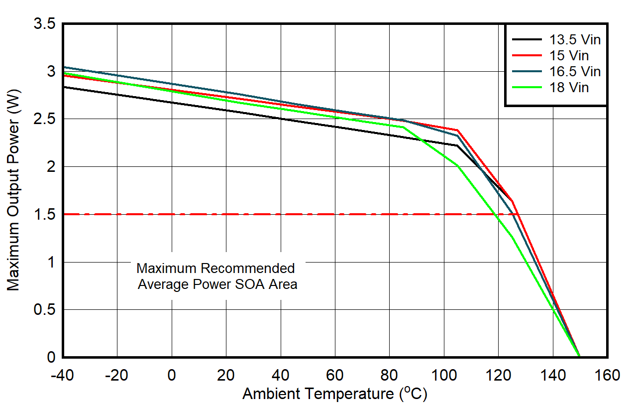 Figure 6-5 SOA Derating Curves:
VVDD-VEE = 25V, VCOM-VEE = 5V,
Tshut=160oC, No Load on
VCOM-VEE
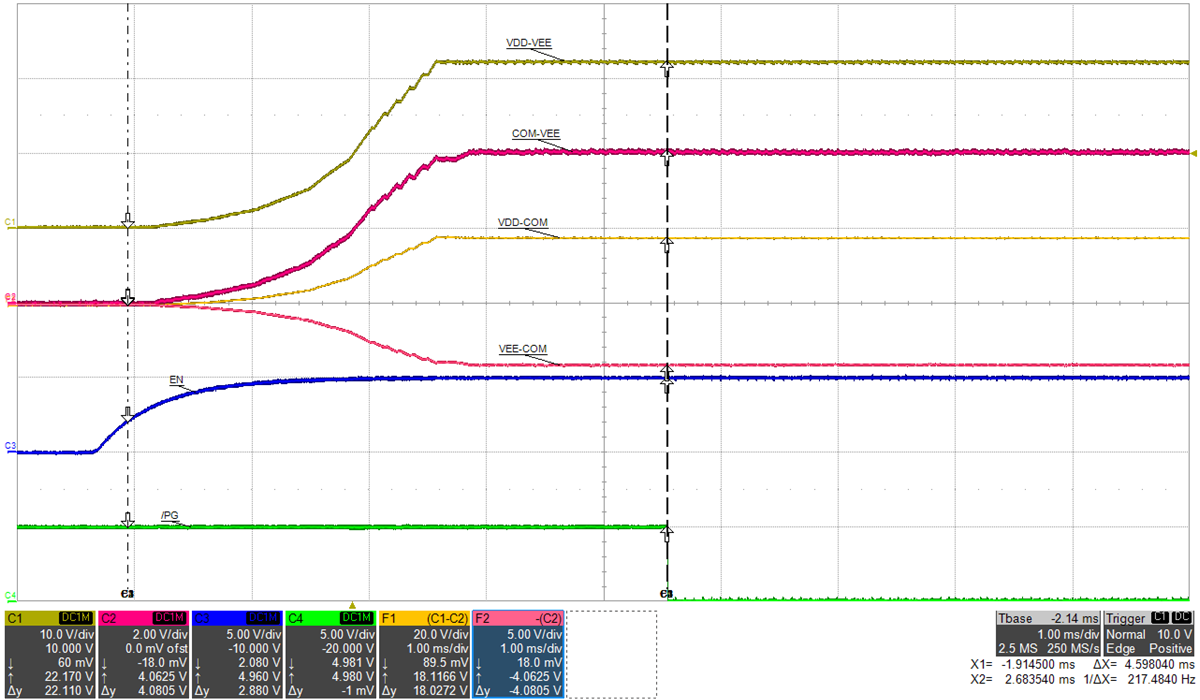 Figure 6-7 Start-up: VIN = 15V, VVDD-VEE = 22V,
VCOM-VEE = 4V, IVDD-VEE = 68mA, No Load on
VCOM-VEE. Time Scale: 1ms/div.
 Figure 6-9 Load
Transient Response: Between No Load and 1.5W, VIN = 15V,
VVDD-VEE = 22V, VCOM-VEE = 4V
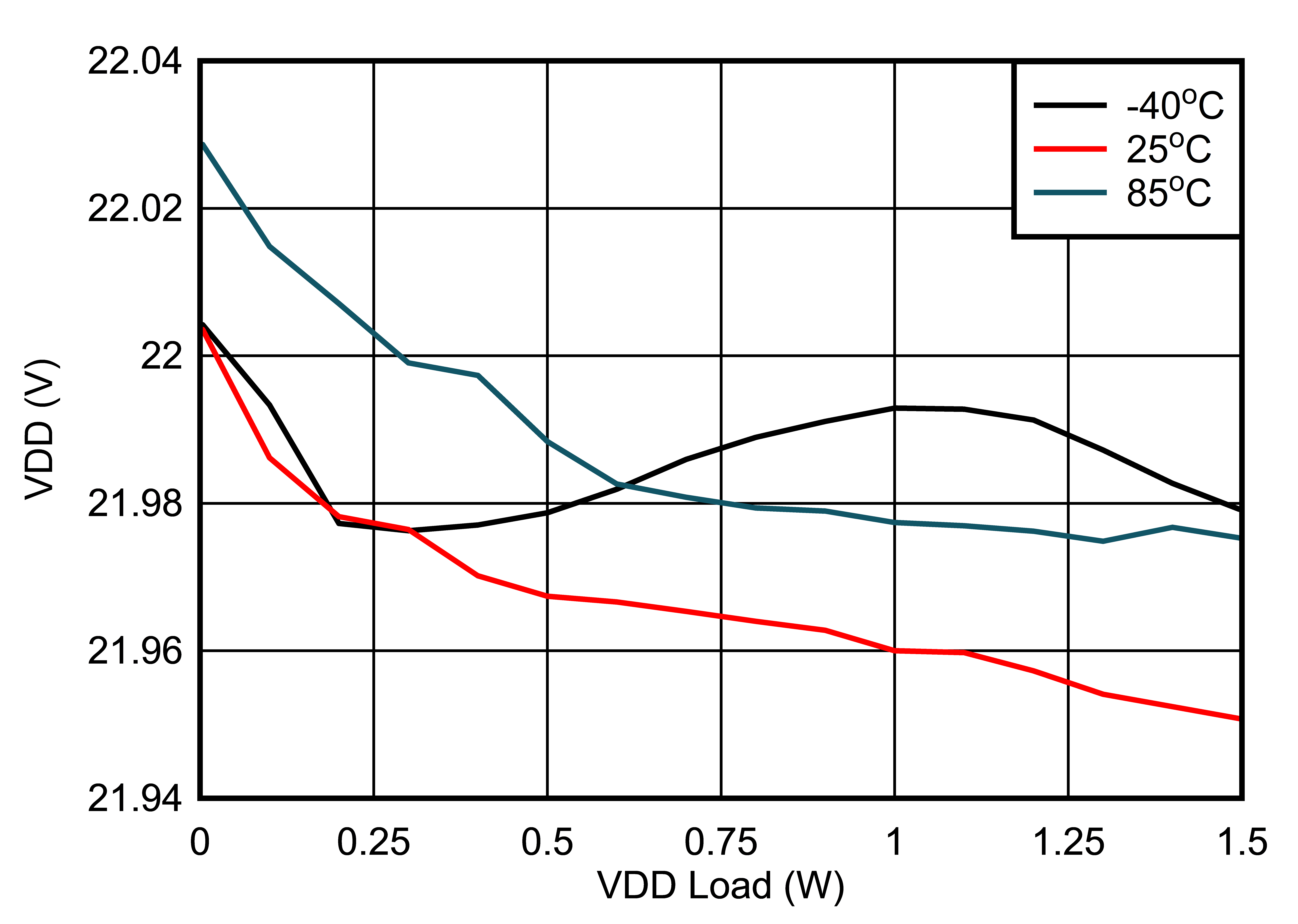 Figure 6-11 VVDD-VEE Load Regulation: VIN = 15V,
VVDD-VEE = 22V, VCOM-VEE = 4V
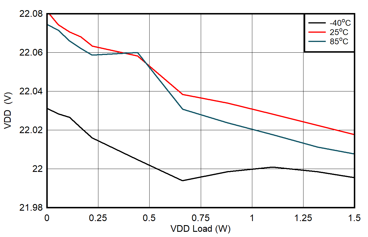 Figure 6-13 VVDD-VEE Load Regulation: VIN = 18V,
VVDD-VEE = 22V, VCOM-VEE = 4V
 Figure 6-15 VCOM-VEE Load Regulation: VIN = 15V,
VVDD-VEE = 22V, VCOM-VEE = 4V
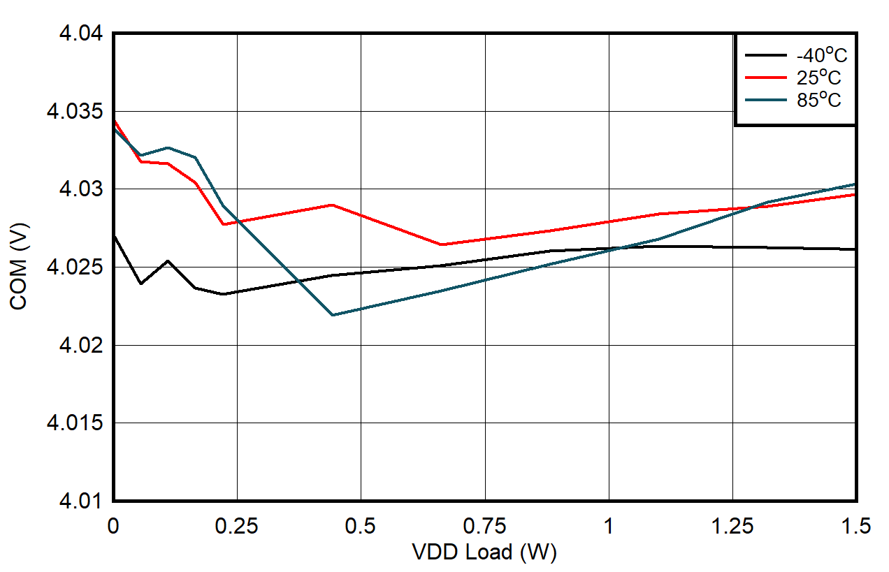 Figure 6-17 VCOM-VEE Load Regulation: VIN = 18V,
VVDD-VEE = 22V, VCOM-VEE = 4V
 Figure 6-19 Efficiency vs. Load on VVDD-VEE: VIN = 15V,
VVDD-VEE = 22V, VCOM-VEE = 4V, No Load on
VCOM-VEE
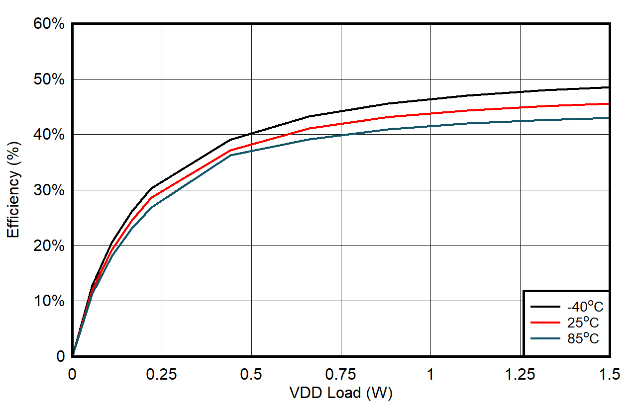 Figure 6-21 Efficiency vs. Load on VVDD-VEE: VIN = 18V,
VVDD-VEE = 22V, VCOM-VEE = 4V, No Load on
VCOM-VEE
 Figure 6-23 Input
Current vs. Load on VVDD-VEE: VIN = 15V,
VVDD-VEE = 22V, VCOM-VEE = 4V, No Load on
VCOM-VEE
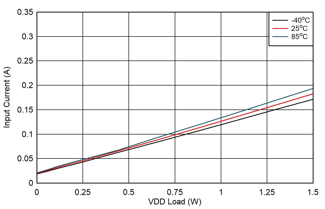 Figure 6-25 Input
Current vs. Load on VVDD-VEE: VIN = 18V,
VVDD-VEE = 22V, VCOM-VEE = 4V, No Load on
VCOM-VEE
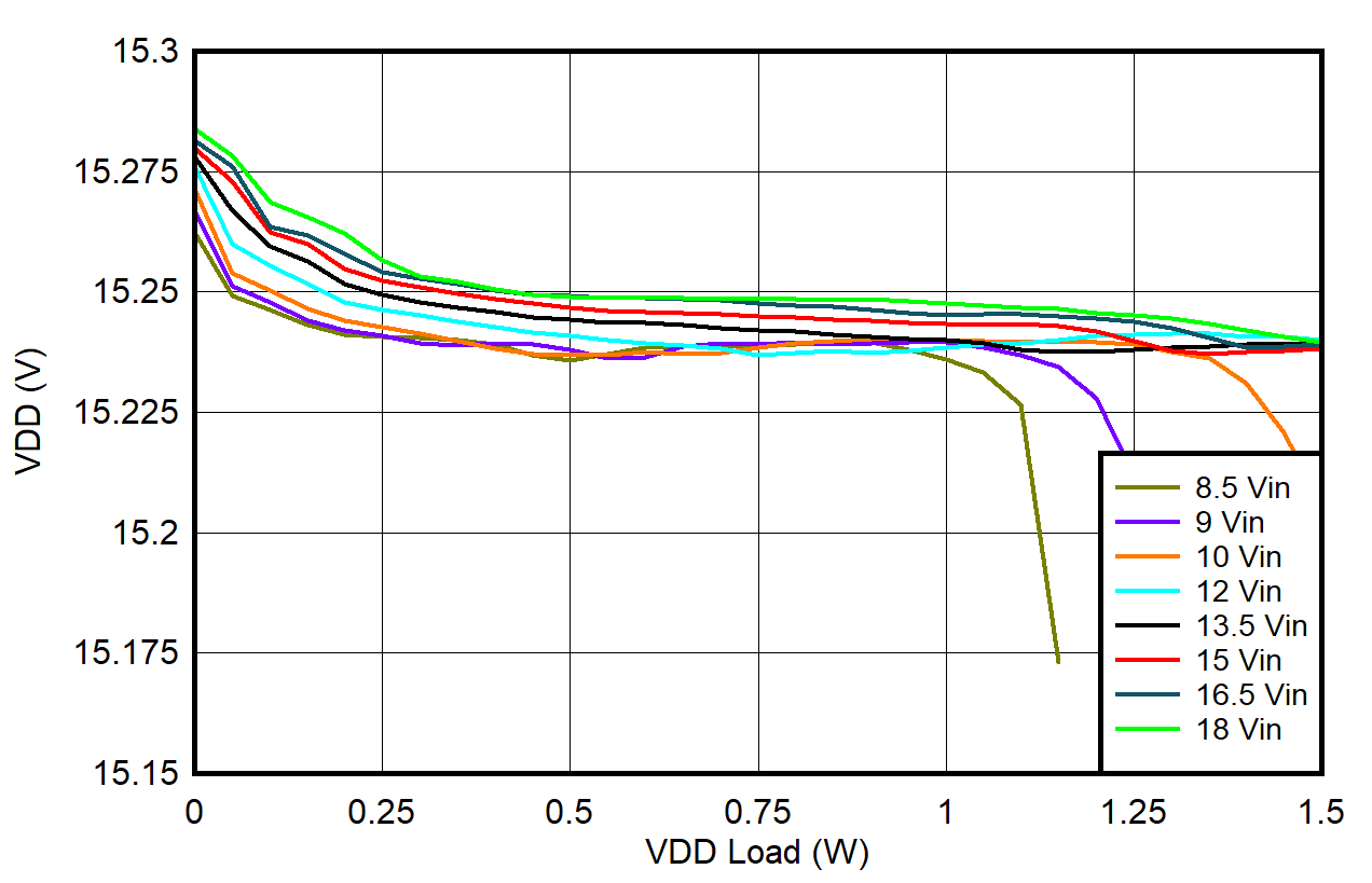 Figure 6-27 UCC14341B-Q1 VVDD-VEE Load Regulation: TAMBIENT =
-40oC, VVDD-VEE = 15V, VCOM-VEE =
4V
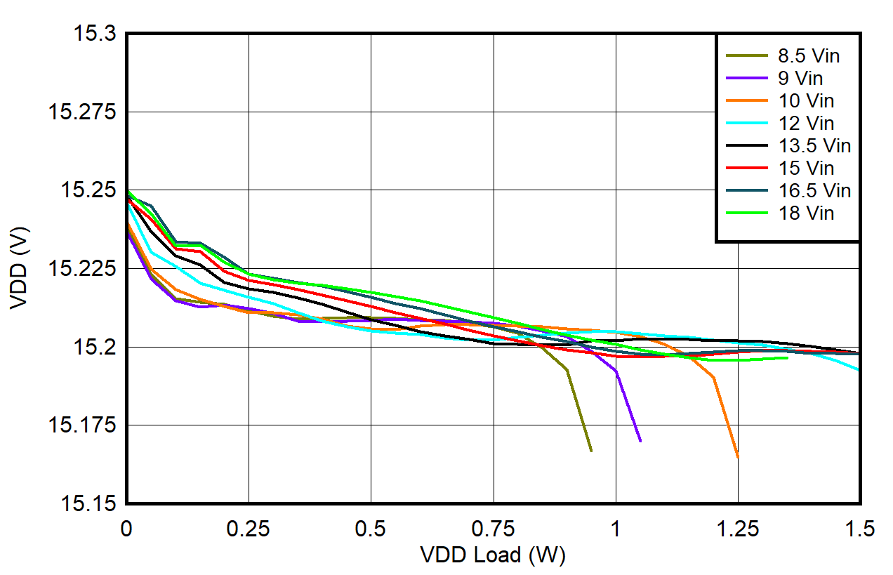 Figure 6-29 UCC14341B-Q1 VVDD-VEE Load Regulation: TAMBIENT =
85oC, VVDD-VEE = 15V, VCOM-VEE =
4V
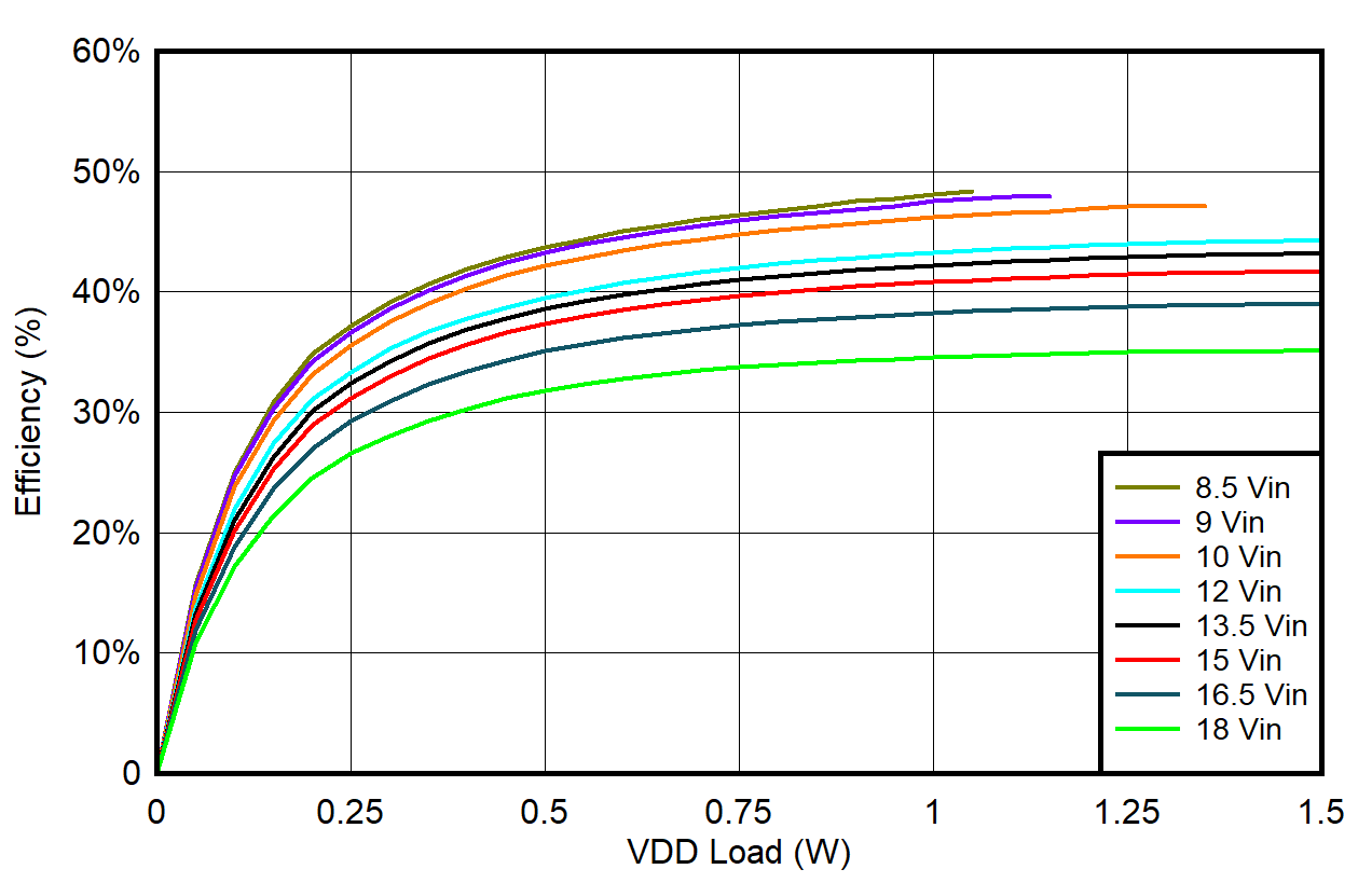 Figure 6-31 UCC14341B-Q1 Efficiency vs. Load on VVDD-VEE:
TAMBIENT = 25oC, VVDD-VEE = 15V,
VCOM-VEE = 4V, No Load on VCOM-VEE
 Figure 6-2 SOA
Derating Curves: VVDD-VEE = 15V, VCOM-VEE = 5V,
Tshut=160oC, No Load on
VCOM-VEE
 Figure 6-4 SOA
Derating Curves: VVDD-VEE = 22V, VCOM-VEE = 4V,
Tshut=160oC, No Load on
VCOM-VEE
 Figure 6-6 SOA Derating Curves:
VVDD-VEE = 22V, VCOM-VEE = 4V,
Tshut=150oC, No Load on VCOM-VEE,
tested in a shielded box.
 Figure 6-8 Shutdown: VIN = 15V, VVDD-VEE = 22V,
VCOM-VEE = 4V, IVDD-VEE = 68mA, No Load on
VCOM-VEE. Time Scale: 2ms/div.
 Figure 6-10 VVDD-VEE Load Regulation: VIN = 13.5V,
VVDD-VEE = 22V, VCOM-VEE = 4V
 Figure 6-12 VVDD-VEE Load Regulation: VIN = 16.5V,
VVDD-VEE = 22V, VCOM-VEE = 4V
 Figure 6-14 VCOM-VEE Load Regulation: VIN = 13.5V,
VVDD-VEE = 22V, VCOM-VEE = 4V
 Figure 6-16 VCOM-VEE Load Regulation: VIN = 16.5V,
VVDD-VEE = 22V, VCOM-VEE = 4V
 Figure 6-18 Efficiency vs. Load on VVDD-VEE: VIN = 13.5V,
VVDD-VEE = 22V, VCOM-VEE = 4V, No Load on
VCOM-VEE
 Figure 6-20 Efficiency vs. Load on VVDD-VEE: VIN = 16.5V,
VVDD-VEE = 22V, VCOM-VEE = 4V, No Load on
VCOM-VEE
 Figure 6-22 Input
Current vs. Load on VVDD-VEE: VIN = 13.5V,
VVDD-VEE = 22V, VCOM-VEE = 4V, No Load on
VCOM-VEE
 Figure 6-24 Input
Current vs. Load on VVDD-VEE: VIN = 16.5V,
VVDD-VEE = 22V, VCOM-VEE = 4V, No Load on
VCOM-VEE
 Figure 6-26 UCC14341B-Q1 SOA Derating Curves: VVDD-VEE = 15V,
VCOM-VEE = 5V, Tshut=160oC, No Load on
VCOM-VEE
 Figure 6-28 UCC14341B-Q1 VVDD-VEE Load Regulation: TAMBIENT =
25oC, VVDD-VEE = 15V, VCOM-VEE =
4V
 Figure 6-30 UCC14341B-Q1 Efficiency vs. Load on VVDD-VEE:
TAMBIENT = -40oC, VVDD-VEE = 15V,
VCOM-VEE = 4V, No Load on VCOM-VEE
 Figure 6-32 UCC14341B-Q1 Efficiency vs. Load on VVDD-VEE:
TAMBIENT = 85oC, VVDD-VEE = 15V,
VCOM-VEE = 4V, No Load on VCOM-VEE
 Figure 6-3 SOA
Derating Curves: VVDD-VEE = 18V, VCOM-VEE = 3V,
Tshut=160oC, No Load on
VCOM-VEE
 Figure 6-5 SOA Derating Curves:
VVDD-VEE = 25V, VCOM-VEE = 5V,
Tshut=160oC, No Load on
VCOM-VEE
 Figure 6-7 Start-up: VIN = 15V, VVDD-VEE = 22V,
VCOM-VEE = 4V, IVDD-VEE = 68mA, No Load on
VCOM-VEE. Time Scale: 1ms/div.
 Figure 6-9 Load
Transient Response: Between No Load and 1.5W, VIN = 15V,
VVDD-VEE = 22V, VCOM-VEE = 4V
 Figure 6-11 VVDD-VEE Load Regulation: VIN = 15V,
VVDD-VEE = 22V, VCOM-VEE = 4V
 Figure 6-13 VVDD-VEE Load Regulation: VIN = 18V,
VVDD-VEE = 22V, VCOM-VEE = 4V
 Figure 6-15 VCOM-VEE Load Regulation: VIN = 15V,
VVDD-VEE = 22V, VCOM-VEE = 4V
 Figure 6-17 VCOM-VEE Load Regulation: VIN = 18V,
VVDD-VEE = 22V, VCOM-VEE = 4V
 Figure 6-19 Efficiency vs. Load on VVDD-VEE: VIN = 15V,
VVDD-VEE = 22V, VCOM-VEE = 4V, No Load on
VCOM-VEE
 Figure 6-21 Efficiency vs. Load on VVDD-VEE: VIN = 18V,
VVDD-VEE = 22V, VCOM-VEE = 4V, No Load on
VCOM-VEE
 Figure 6-23 Input
Current vs. Load on VVDD-VEE: VIN = 15V,
VVDD-VEE = 22V, VCOM-VEE = 4V, No Load on
VCOM-VEE
 Figure 6-25 Input
Current vs. Load on VVDD-VEE: VIN = 18V,
VVDD-VEE = 22V, VCOM-VEE = 4V, No Load on
VCOM-VEE
 Figure 6-27 UCC14341B-Q1 VVDD-VEE Load Regulation: TAMBIENT =
-40oC, VVDD-VEE = 15V, VCOM-VEE =
4V
 Figure 6-29 UCC14341B-Q1 VVDD-VEE Load Regulation: TAMBIENT =
85oC, VVDD-VEE = 15V, VCOM-VEE =
4V
 Figure 6-31 UCC14341B-Q1 Efficiency vs. Load on VVDD-VEE:
TAMBIENT = 25oC, VVDD-VEE = 15V,
VCOM-VEE = 4V, No Load on VCOM-VEE