SLUSF14 august 2023 UCC15241-Q1
PRODUCTION DATA
- 1
- 1 Features
- 2 Applications
- 3 Description
- 4 Revision History
- 5 Device Comparison
- 6 Pin Configuration and Functions
- 7 Specifications
- 8 Safety-Related Certifications
- 9 Insulation Characteristics
- 10Typical Characteristics
- 11Detailed Description
- 12Application and Implementation
- 13Device and Documentation Support
- 14Mechanical, Packaging, and Orderable Information
- 15Tape and Reel Information
Package Options
Mechanical Data (Package|Pins)
- DWN|36
Thermal pad, mechanical data (Package|Pins)
Orderable Information
12.2.3 Application Curves
The UCC15241-Q1 has the same pinout and functionality as the UCC14240-Q1, with a different maximum output power capability. The application response will be similar and the PMP23223 reference design is still valuable to demonstrate the capability. The PMP23223 is a reference design that pairs the complementary UCC14240-Q1 isolated DC/DC power module with the UCC21732-Q1 isolated gate driver for a SiC power MOSFET or IGBT power module. The following waveforms show the controlled soft start for both positive and negative rails. Also shown, is the fast and highly accurate voltage regulation during gate driver switching from 1 kHz to 35 kHz. See PMP23223 reference design test report for more details.
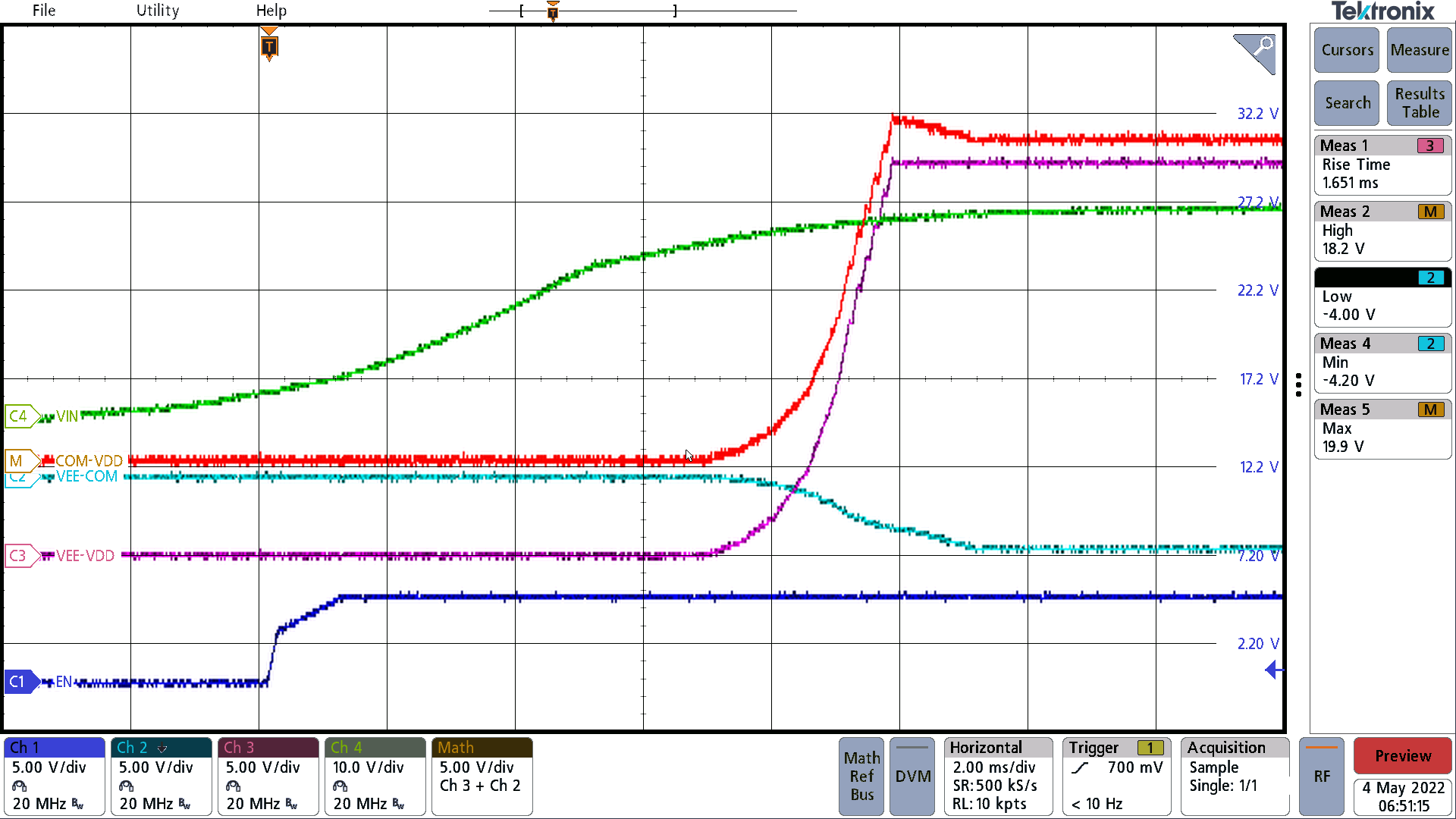 Figure 12-11 Power-Up Sequence.
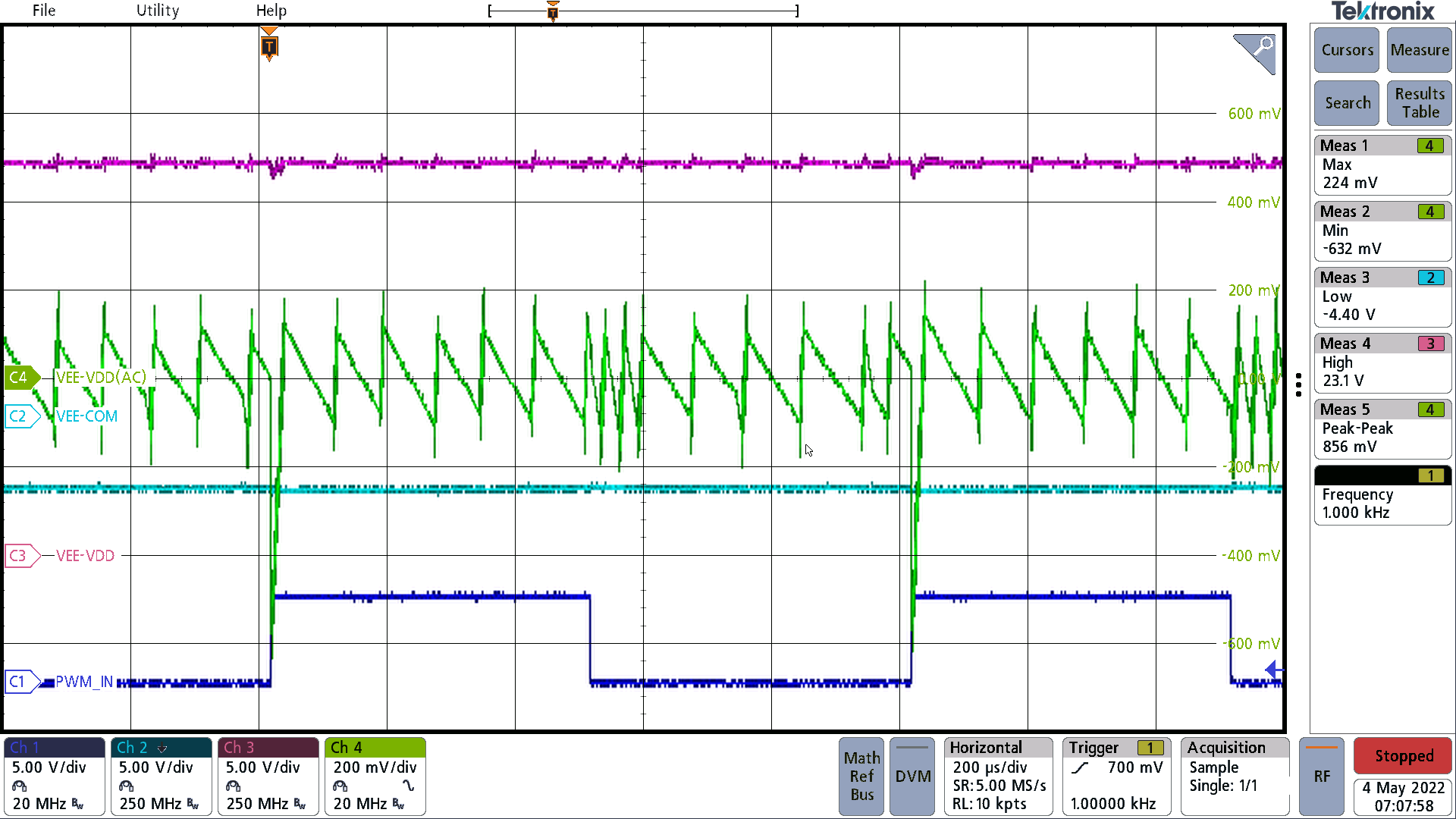 Figure 12-13 Ripple voltage: VDD-VEE Switching 100-nF Load at 1 kHz.
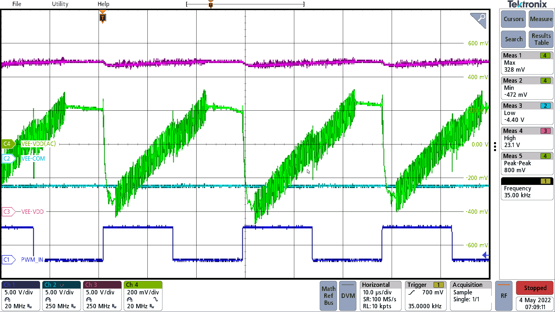 Figure 12-15 Ripple voltage: VDD-VEE Switching 100-nF Load at 35 kHz.
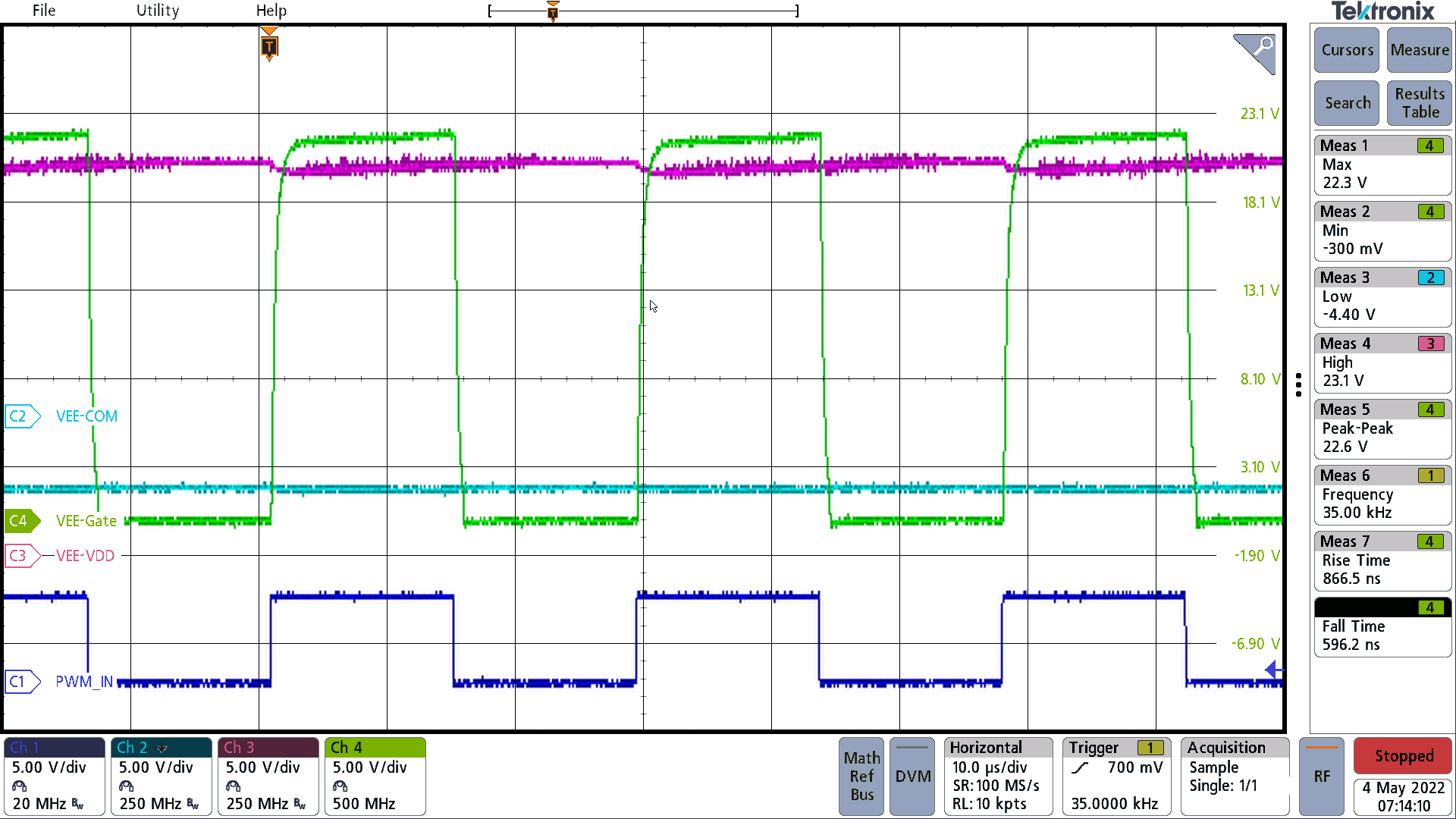 Figure 12-17 Gate Waveform Switching 100 nF at 35kHz.
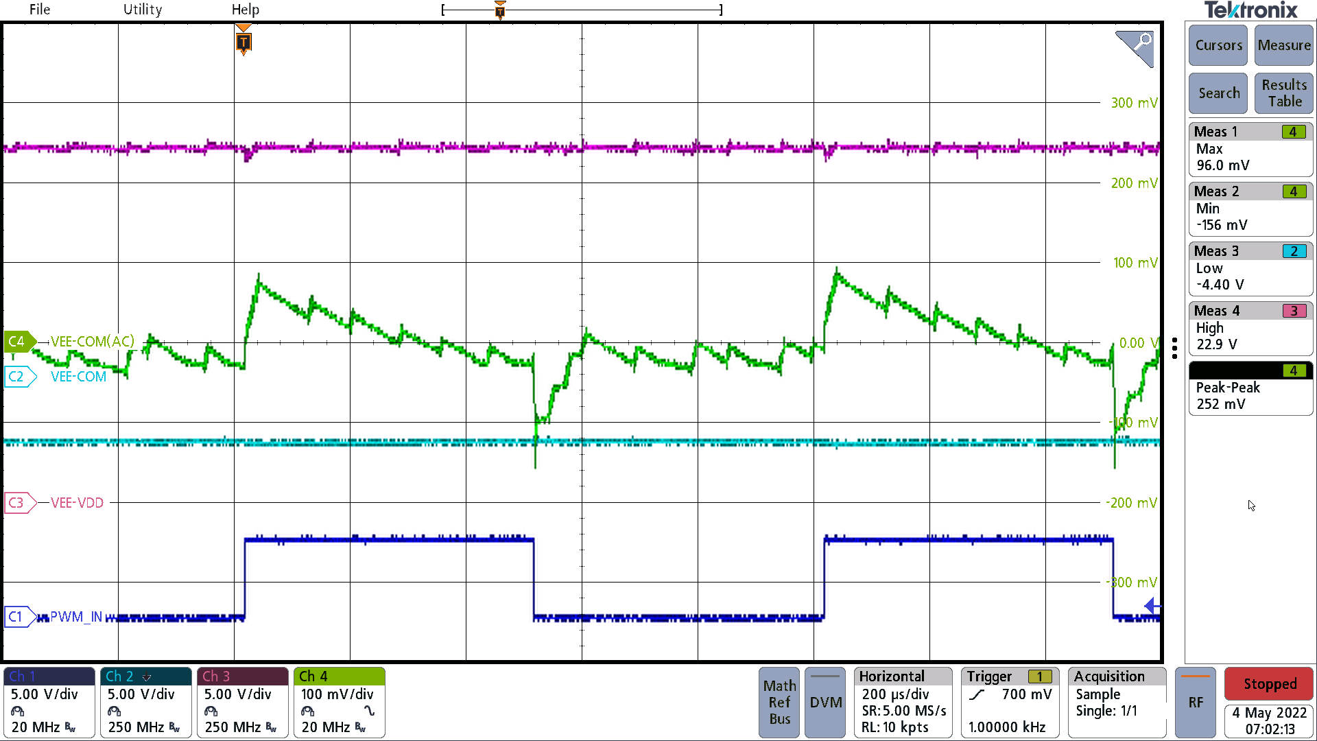 Figure 12-12 Ripple voltage: VEE-COM Switching 100-nF Load at 1 kHz.
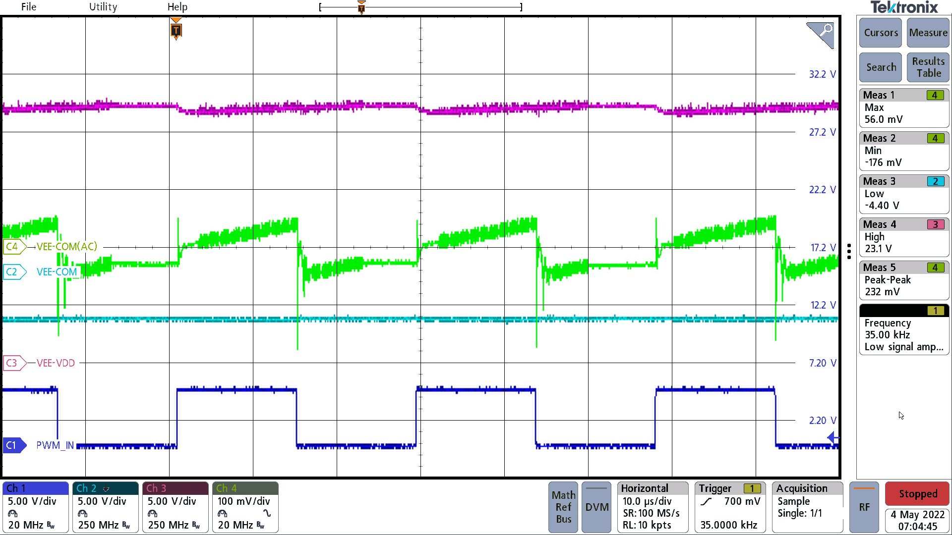 Figure 12-14 Ripple voltage: VEE-COM Switching 100-nF Load at 35 kHz.
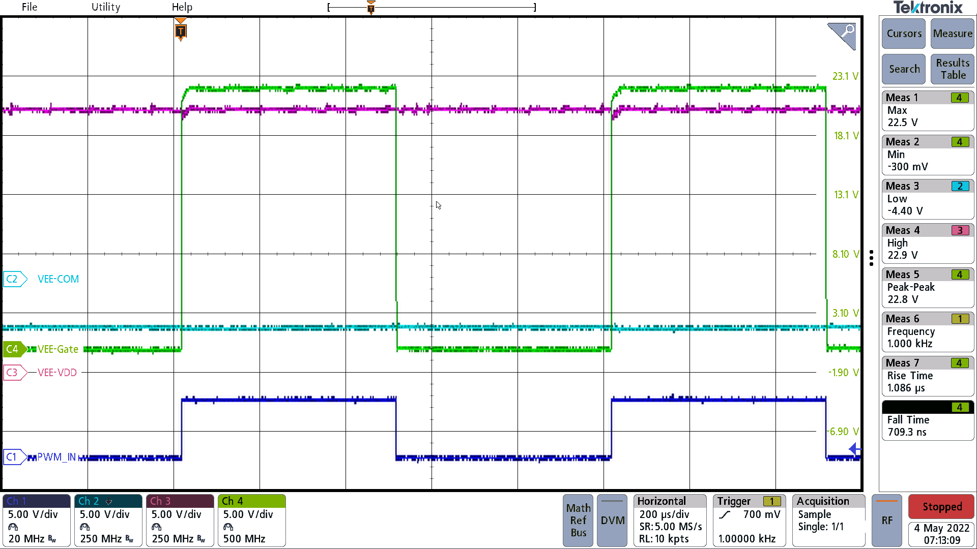 Figure 12-16 Gate Waveform Switching 100 nF at 1 kHz.