SLUSCK0G November   2017  – November 2024 UCC21220 , UCC21220A

PRODUCTION DATA  

  1.   1
  2. Features
  3. Applications
  4. Description
  5. Device Comparison Table
  6. Pin Configuration and Functions
  7. Specifications
    1. 6.1  Absolute Maximum Ratings
    2. 6.2  ESD Ratings
    3. 6.3  Recommended Operating Conditions
    4. 6.4  Thermal Information
    5. 6.5  Power Ratings
    6. 6.6  Insulation Specifications
    7. 6.7  Safety-Limiting Values
    8. 6.8  Electrical Characteristics
    9. 6.9  Switching Characteristics
    10. 6.10 Thermal Derating Curves
    11. 6.11 Typical Characteristics
  8. Parameter Measurement Information
    1. 7.1 Minimum Pulses
    2. 7.2 Propagation Delay and Pulse Width Distortion
    3. 7.3 Rising and Falling Time
    4. 7.4 Input and Disable Response Time
    5. 7.5 Power-up UVLO Delay to OUTPUT
    6. 7.6 CMTI Testing
  9. Detailed Description
    1. 8.1 Overview
    2. 8.2 Functional Block Diagram
    3. 8.3 Feature Description
      1. 8.3.1 VDD, VCCI, and Under Voltage Lock Out (UVLO)
      2. 8.3.2 Input and Output Logic Table
      3. 8.3.3 Input Stage
      4. 8.3.4 Output Stage
      5. 8.3.5 Diode Structure in UCC21220 and UCC21220A
    4. 8.4 Device Functional Modes
      1. 8.4.1 Disable Pin
  10. Application and Implementation
    1. 9.1 Application Information
    2. 9.2 Typical Application
      1. 9.2.1 Design Requirements
      2. 9.2.2 Detailed Design Procedure
        1. 9.2.2.1 Designing INA/INB Input Filter
        2. 9.2.2.2 Select External Bootstrap Diode and its Series Resistor
        3. 9.2.2.3 Gate Driver Output Resistor
        4. 9.2.2.4 Estimating Gate Driver Power Loss
        5. 9.2.2.5 Estimating Junction Temperature
        6. 9.2.2.6 Selecting VCCI, VDDA/B Capacitor
          1. 9.2.2.6.1 Selecting a VCCI Capacitor
          2. 9.2.2.6.2 Selecting a VDDA (Bootstrap) Capacitor
          3. 9.2.2.6.3 Select a VDDB Capacitor
        7. 9.2.2.7 Application Circuits with Output Stage Negative Bias
      3. 9.2.3 Application Curves
  11. 10Power Supply Recommendations
  12. 11Layout
    1. 11.1 Layout Guidelines
      1. 11.1.1 Component Placement Considerations
      2. 11.1.2 Grounding Considerations
      3. 11.1.3 High-Voltage Considerations
      4. 11.1.4 Thermal Considerations
    2. 11.2 Layout Example
  13. 12Device and Documentation Support
    1. 12.1 Third-Party Products Disclaimer
    2. 12.2 Documentation Support
      1. 12.2.1 Related Documentation
    3. 12.3 Receiving Notification of Documentation Updates
    4. 12.4 Support Resources
    5. 12.5 Trademarks
    6. 12.6 Electrostatic Discharge Caution
    7. 12.7 Glossary
  14. 13Revision History
  15. 14Mechanical, Packaging, and Orderable Information

Package Options

Refer to the PDF data sheet for device specific package drawings

Mechanical Data (Package|Pins)
  • D|16
Thermal pad, mechanical data (Package|Pins)
Orderable Information

Typical Application

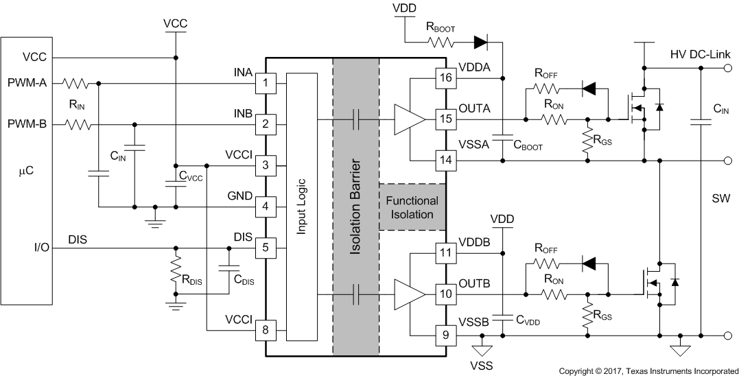
The circuit in Figure 9-1 shows a reference design with UCC21220 or UCC21220A driving a typical half-bridge configuration which could be used in several popular power converter topologies such as synchronous buck, synchronous boost, half-bridge/full bridge isolated topologies, and 3-phase motor drive applications.
UCC21220 UCC21220A Typical Application SchematicFigure 9-1 Typical Application Schematic