SLUSCV6A April 2017 – February 2018 UCC21225A
PRODUCTION DATA.
- 1 Features
- 2 Applications
- 3 Description
- 4 Revision History
- 5 Pin Configuration and Functions
-
6 Specifications
- 6.1 Absolute Maximum Ratings
- 6.2 ESD Ratings
- 6.3 Recommended Operating Conditions
- 6.4 Thermal Information
- 6.5 Power Ratings
- 6.6 Insulation Specifications
- 6.7 Safety-Related Certifications
- 6.8 Safety-Limiting Values
- 6.9 Electrical Characteristics
- 6.10 Switching Characteristics
- 6.11 Insulation Characteristics and Thermal Derating Curves
- 6.12 Typical Characteristics
- 7 Parameter Measurement Information
- 8 Detailed Description
-
9 Application and Implementation
- 9.1 Application Information
- 9.2
Typical Application
- 9.2.1 Design Requirements
- 9.2.2
Detailed Design Procedure
- 9.2.2.1 Designing INA/INB Input Filter
- 9.2.2.2 Select External Bootstrap Diode and Series Resistor
- 9.2.2.3 Gate Driver Output Resistor
- 9.2.2.4 Estimate Gate Driver Power Loss
- 9.2.2.5 Estimating Junction Temperature
- 9.2.2.6 Selecting VCCI, VDDA/B Capacitor
- 9.2.2.7 Dead Time Setting Guidelines
- 9.2.2.8 Application Circuits with Output Stage Negative Bias
- 9.2.3 Application Curves
- 10Power Supply Recommendations
- 11Layout
- 12Device and Documentation Support
- 13Mechanical, Packaging, and Orderable Information
Package Options
Mechanical Data (Package|Pins)
- NPL|13
Thermal pad, mechanical data (Package|Pins)
Orderable Information
11.2 Layout Example
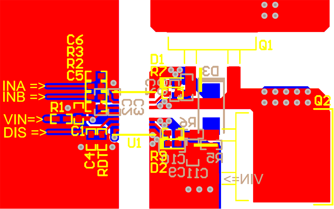
Figure 41 shows a 2-layer PCB layout example with the signals and key components labeled.
 Figure 41. Layout Example
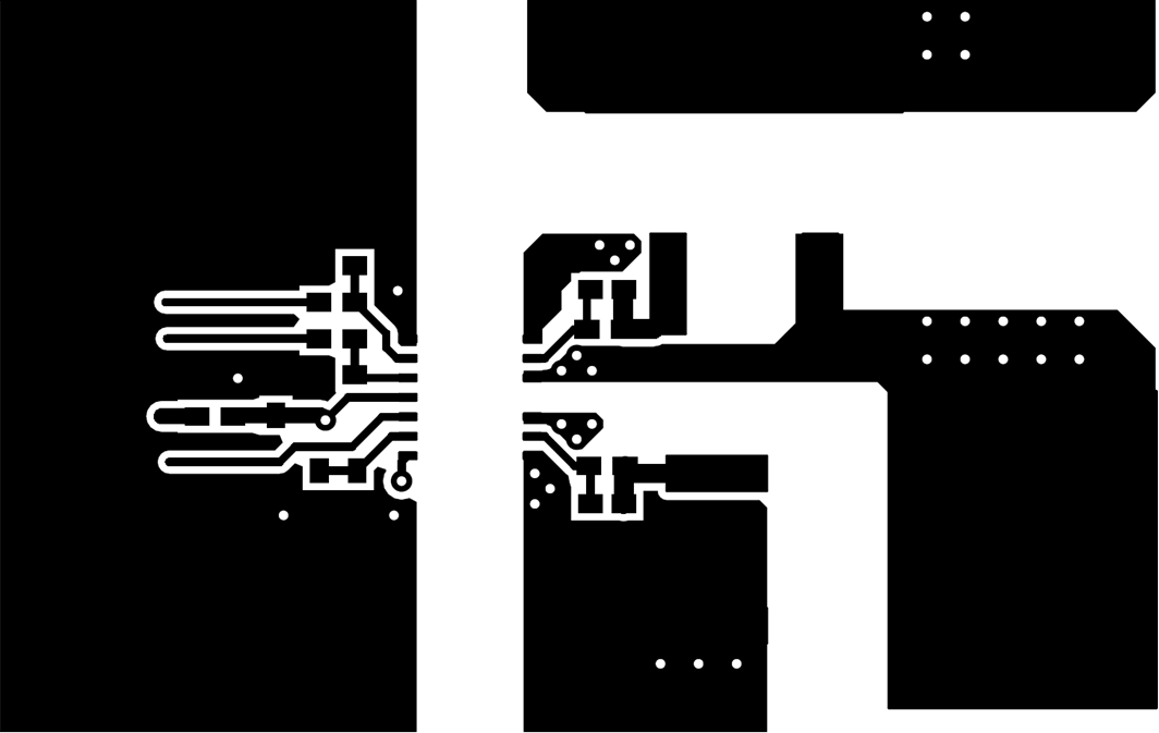
Figure 42 and Figure 43 shows top and bottom layer traces and copper.
NOTE
There are no PCB traces or copper between the primary and secondary side, which ensures isolation performance.
PCB trace spacing between the high-side and low-side gate drivers in the output stage are increased to minimize cross-talk due to parasitic capacitance coupling between the switching node VSSA (SW), where high dv/dt may exist, and the low-side gate drive circuit.


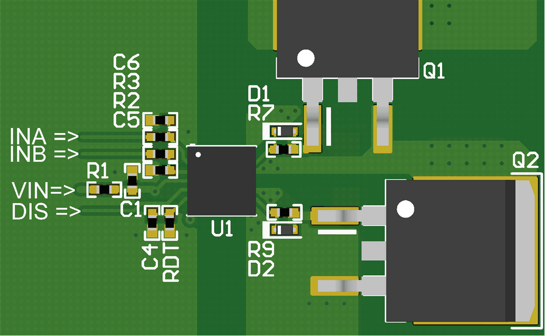
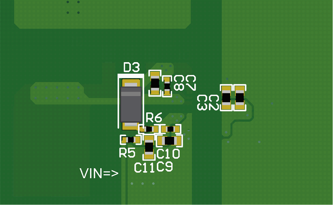
Figure 44 and Figure 45 are 3D layout pictures with top view and bottom views.
NOTE
The location of the PCB cutout between the primary side and secondary sides, which ensures isolation performance.

