SLUSF46A April 2024 – June 2024 UCC21231
PRODUCTION DATA
- 1
- 1 Features
- 2 Applications
- 3 Description
- 4 Pin Configuration and Functions
-
5 Specifications
- 5.1 Absolute Maximum Ratings
- 5.2 ESD Ratings
- 5.3 Recommended Operating Conditions
- 5.4 Thermal Information
- 5.5 Power Ratings
- 5.6 Insulation Specifications
- 5.7 Safety Limiting Values
- 5.8 Electrical Characteristics
- 5.9 Switching Characteristics
- 5.10 Insulation Characteristics Curves
- 5.11 Typical Characteristics
- 6 Parameter Measurement Information
- 7 Detailed Description
-
8 Application and Implementation
- 8.1 Application Information
- 8.2
Typical Application
- 8.2.1 Design Requirements
- 8.2.2
Detailed Design Procedure
- 8.2.2.1 Designing INA/INB Input Filter
- 8.2.2.2 Select External Bootstrap Diode and its Series Resistor
- 8.2.2.3 Gate Driver Output Resistor
- 8.2.2.4 Gate to Source Resistor Selection
- 8.2.2.5 Estimate Gate Driver Power Loss
- 8.2.2.6 Estimating Junction Temperature
- 8.2.2.7 Selecting VCCI, VDDA/B Capacitor
- 8.2.2.8 Dead Time Setting Guidelines
- 8.2.2.9 Application Circuits with Output Stage Negative Bias
- 8.2.3 Application Curves
- 9 Power Supply Recommendations
- 10Layout
- 11Device and Documentation Support
- 12Revision History
- 13Mechanical, Packaging, and Orderable Information
Package Options
Refer to the PDF data sheet for device specific package drawings
Mechanical Data (Package|Pins)
- DLG|13
Thermal pad, mechanical data (Package|Pins)
Orderable Information
4 Pin Configuration and Functions
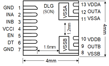
 Figure 4-1 DLG
Package13-Pin SONTop View
Figure 4-1 DLG
Package13-Pin SONTop ViewTable 4-1 Pin Functions
| PIN | TYPE(1) | DESCRIPTION | |
|---|---|---|---|
| NAME | NO. | ||
| INA | 2 | I | Input signal for A channel. INA input has a TTL/CMOS compatible input threshold. This pin is pulled low internally if left open. It is recommended to use an RC filter on INA, with R = 10 Ω to 100 Ω and C = 10 pF to 100 pF. |
| INB | 3 | I | Input signal for B channel. INB input has a TTL/CMOS compatible input threshold. This pin is pulled low internally if left open. It is recommended to use an RC filter on INB, with R = 10 Ω to 100 Ω and C = 10 pF to 100 pF. |
| VCCI | 4 | P | Primary-side supply voltage. Locally decoupled to GND using a low ESR/ESL capacitor located as close to the device as possible. |
| GND | 1, 7 | G | Primary-side ground reference. All signals in the primary side are referenced to this ground. |
| EN | 5 | I | Enable both driver outputs if asserted high, disable the output if set low. It is recommended to tie this pin to VCCI if not used to achieve better noise immunity. This pin is internally pulled low if left floating. It is recommended to use an RC filter on EN, with R = 0 Ω to 100 Ω and C = 100 pF to 1000 pF. |
| DT | 6 | I | DT
pin configurations:
|
| VDDA | 13 | P | Secondary-side power for driver A. Locally decoupled to VSSA using a low ESR/ESL capacitor located as close to the device as possible. |
| OUTA | 12 | O | Output of driver A. Connect to the gate of the A channel transistor. |
| VSSA | 11 | G | Ground for secondary-side driver A. Ground reference for secondary side A channel. |
| VDDB | 10 | P | Secondary-side power for driver B. Locally decoupled to VSSB using low ESR/ESL capacitor located as close to the device as possible. |
| OUTB | 9 | O | Output of driver B. Connect to the gate of the B channel transsitor. |
| VSSB | 8 | G | Ground for secondary-side driver B. Ground reference for secondary side B channel. |
(1) P =Power, G= Ground, I= Input, O= Output