SLUSDU7A March 2020 – August 2024 UCC21320-Q1
PRODUCTION DATA
- 1
- 1 Features
- 2 Applications
- 3 Description
- 4 Pin Configuration and Functions
-
5 Specifications
- 5.1 Absolute Maximum Ratings
- 5.2 ESD Ratings (Automotive)
- 5.3 Recommended Operating Conditions
- 5.4 Thermal Information
- 5.5 Power Ratings
- 5.6 Insulation Specifications
- 5.7 Safety Limiting Values
- 5.8 Electrical Characteristics
- 5.9 Timing Requirements
- 5.10 Switching Characteristics
- 5.11 Insulation Characteristics Curves
- 5.12 Typical Characteristics
- 6 Parameter Measurement Information
- 7 Detailed Description
-
8 Application and Implementation
- 8.1 Application Information
- 8.2
Typical Application
- 8.2.1 Design Requirements
- 8.2.2
Detailed Design Procedure
- 8.2.2.1 Designing INA/INB Input Filter
- 8.2.2.2 Select External Bootstrap Diode and its Series Resistor
- 8.2.2.3 Gate Driver Output Resistor
- 8.2.2.4 Gate to Source Resistor Selection
- 8.2.2.5 Estimate Gate Driver Power Loss
- 8.2.2.6 Estimating Junction Temperature
- 8.2.2.7 Selecting VCCI, VDDA/B Capacitor
- 8.2.2.8 Dead Time Setting Guidelines
- 8.2.2.9 Application Circuits with Output Stage Negative Bias
- 8.2.3 Application Curves
- 9 Power Supply Recommendations
- 10Layout
- 11Device and Documentation Support
- 12Revision History
- 13Mechanical, Packaging, and Orderable Information
Package Options
Refer to the PDF data sheet for device specific package drawings
Mechanical Data (Package|Pins)
- DWK|14
Thermal pad, mechanical data (Package|Pins)
Orderable Information
3 Description
The UCC21320-Q1 is an isolated dual-channel gate driver with 4A source and 6A sink peak current. It is designed to drive power MOSFETs, IGBTs, and SiC MOSFETs up to 5MHz.
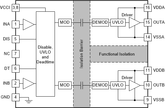
The input side is isolated from the two output drivers by a 3.75kVRMS basic isolation barrier, with a minimum of 125V/ns common-mode transient immunity (CMTI). Internal functional isolation between the two secondary-side drivers allows a working voltage of up to 1500VDC.
Every driver can be configured as two low-side drivers, two high-side drivers, or a half-bridge driver with programmable dead time (DT). A disable pin shuts down both outputs simultaneously, and allows normal operation when left open or grounded. As a fail-safe measure, primary-side logic failures force both outputs low.
Each device accepts VDD supply voltages up to 25V. A wide input VCCI range from 3V to 18V makes the driver suitable for interfacing with both analog and digital controllers. All supply voltage pins have under voltage lock-out (UVLO) protection.
With all these advanced features, the UCC21320-Q1 enables high efficiency, high power density, and robustness.
| PART NUMBER | PACKAGE | BODY SIZE (NOM) |
|---|---|---|
| UCC21320DWK-Q1 | DWK (SOIC 14) | 10.30mm × 7.50mm |
 Functional Block Diagram