SLUSDU7A March 2020 – August 2024 UCC21320-Q1
PRODUCTION DATA
- 1
- 1 Features
- 2 Applications
- 3 Description
- 4 Pin Configuration and Functions
-
5 Specifications
- 5.1 Absolute Maximum Ratings
- 5.2 ESD Ratings (Automotive)
- 5.3 Recommended Operating Conditions
- 5.4 Thermal Information
- 5.5 Power Ratings
- 5.6 Insulation Specifications
- 5.7 Safety Limiting Values
- 5.8 Electrical Characteristics
- 5.9 Timing Requirements
- 5.10 Switching Characteristics
- 5.11 Insulation Characteristics Curves
- 5.12 Typical Characteristics
- 6 Parameter Measurement Information
- 7 Detailed Description
-
8 Application and Implementation
- 8.1 Application Information
- 8.2
Typical Application
- 8.2.1 Design Requirements
- 8.2.2
Detailed Design Procedure
- 8.2.2.1 Designing INA/INB Input Filter
- 8.2.2.2 Select External Bootstrap Diode and its Series Resistor
- 8.2.2.3 Gate Driver Output Resistor
- 8.2.2.4 Gate to Source Resistor Selection
- 8.2.2.5 Estimate Gate Driver Power Loss
- 8.2.2.6 Estimating Junction Temperature
- 8.2.2.7 Selecting VCCI, VDDA/B Capacitor
- 8.2.2.8 Dead Time Setting Guidelines
- 8.2.2.9 Application Circuits with Output Stage Negative Bias
- 8.2.3 Application Curves
- 9 Power Supply Recommendations
- 10Layout
- 11Device and Documentation Support
- 12Revision History
- 13Mechanical, Packaging, and Orderable Information
Package Options
Refer to the PDF data sheet for device specific package drawings
Mechanical Data (Package|Pins)
- DWK|14
Thermal pad, mechanical data (Package|Pins)
Orderable Information
10.2 Layout Example
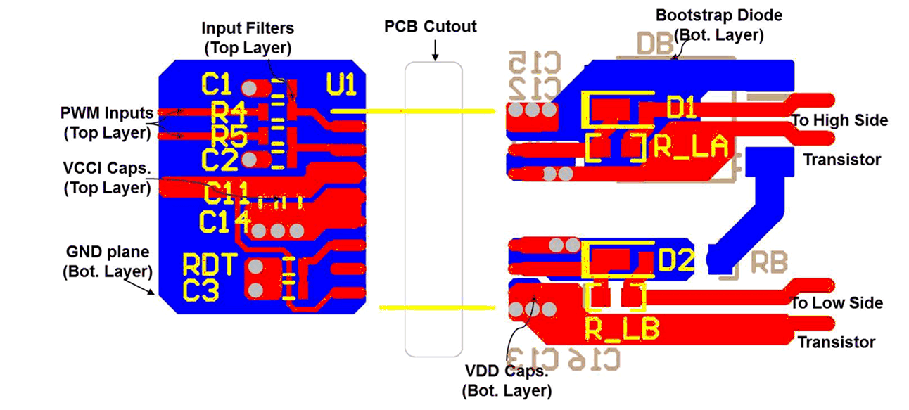
Figure 10-1 shows a 2-layer PCB layout example with the signals and key components labeled.
 Figure 10-1 Layout Example
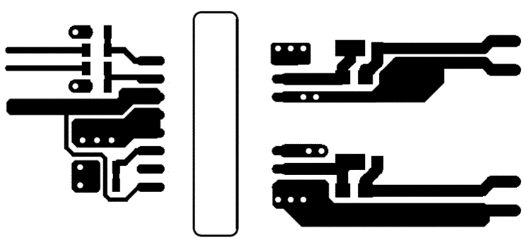
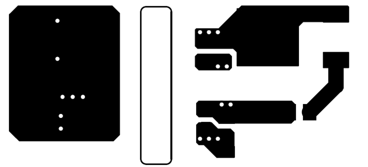
Figure 10-2 and Figure 10-3 shows top and bottom layer traces and copper.
There are no PCB traces or copper between the primary and secondary side, which ensures isolation performance.
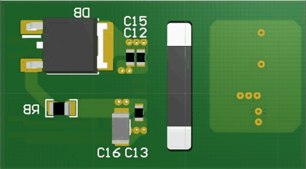
PCB traces between the high-side and low-side gate drivers in the output stage are increased to maximize the creepage distance for high-voltage operation, which will also minimize cross-talk between the switching node VSSA (SW), where high dv/dt may exist, and the low-side gate drive due to the parasitic capacitance coupling. Figure 10-4 shows a 3D view of the bottom side recommended layout, showing the board cutout.


The location of the PCB cutout between the primary side and secondary sides, which ensures isolation performance.
