SLUSF86 May 2024 UCC21331-Q1
PRODUCTION DATA
- 1
- 1 Features
- 2 Applications
- 3 Description
- 4 Pin Configuration and Functions
-
5 Specifications
- 5.1 Absolute Maximum Ratings
- 5.2 ESD Ratings (Automotive)
- 5.3 Recommended Operating Conditions
- 5.4 Thermal Information
- 5.5 Power Ratings
- 5.6 Insulation Specifications
- 5.7 Safety Limiting Values
- 5.8 Electrical Characteristics
- 5.9 Switching Characteristics
- 5.10 Insulation Characteristics Curves
- 5.11 Typical Characteristics
- 6 Parameter Measurement Information
- 7 Detailed Description
-
8 Application and Implementation
- 8.1 Application Information
- 8.2
Typical Application
- 8.2.1 Design Requirements
- 8.2.2
Detailed Design Procedure
- 8.2.2.1 Designing INA/INB Input Filter
- 8.2.2.2 Select External Bootstrap Diode and its Series Resistor
- 8.2.2.3 Gate Driver Output Resistor
- 8.2.2.4 Gate to Source Resistor Selection
- 8.2.2.5 Estimate Gate Driver Power Loss
- 8.2.2.6 Estimating Junction Temperature
- 8.2.2.7 Selecting VCCI, VDDA/B Capacitor
- 8.2.2.8 Dead Time Setting Guidelines
- 8.2.2.9 Application Circuits with Output Stage Negative Bias
- 8.2.3 Application Curves
- 9 Power Supply Recommendations
- 10Layout
- 11Device and Documentation Support
- 12Revision History
- 13Mechanical, Packaging, and Orderable Information
Package Options
Refer to the PDF data sheet for device specific package drawings
Mechanical Data (Package|Pins)
- D|16
Thermal pad, mechanical data (Package|Pins)
Orderable Information
7.3.4 Output Stage
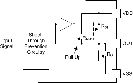
The UCC21331-Q1 output stages feature a pull-up structure which delivers the highest peak-source current when it is most needed, during the Miller plateau region of the power-switch turn on transition (when the power switch drain or collector voltage experiences dV/dt). The output stage pull-up structure features a P-channel MOSFET and an additional Pull-Up N-channel MOSFET in parallel. The function of the N-channel MOSFET is to provide a brief boost in the peak-sourcing current, enabling fast turn on. This is accomplished by briefly turning on the N-channel MOSFET during a narrow instant when the output is changing states from low to high.
The ROH parameter is a DC measurement and it is representative of the on-resistance of the P-channel device only. This is because the Pull-Up N-channel device is held in the off state in DC condition and is turned on only for a brief instant when the output is changing states from low to high. This N-channel device has an on-resistance of approximately 1.47-Ω. Therefore, the effective resistance of the UCC21331-Q1 pull-up stage during this brief turn-on phase is the parallel resistance between the pull-up NMOS and pull-up PMOS, which is 1.47Ω // 5Ω, much lower than what is represented by the ROH parameter. The value of ROH belies the fast nature of the UCC21331-Q1 turn-on time.
The pull-down structure in the UCC21331-Q1 is simply composed of an N-channel MOSFET. The ROL parameter, which is also a DC measurement, is representative of the impedance of the pull-down state in the device. Both outputs of the UCC21331-Q1 are capable of delivering 4-A peak source and 6-A peak sink current pulses. The output voltage swings between VDD and VSS provides rail-to-rail operation, thanks to the MOS-out stage which delivers very low drop-out.
To ensure robust and reliable operation of gate drivers, pay special attention to the minimum pulse width. The minimum pulse width shown in the electrical characteristics table describes the minimum input pulse that would be passed to the output in an unloaded driver. This is dictated by the deglitch filter present in the driver IC. An input ON or OFF pulse width longer than the maximum specification is needed to guarantee an output state change and avoid potential shoot-through. With a loaded driver, extra precaution must be taken to ensure robust operation of the system. During gate switching, if the output state changes before the driver completes each transition, a non-zero current switching event occurs. Combined with layout parasitics, non-zero current switching can cause internal rail overshoot and EOS damage of the gate driver. Thus, a minimum output width is needed for reliable system operation. This minimum output pulse width is dependent on several factors: gate capacitance, VDD supply voltage, gate resistance, and PCB layout parasitics. The minimum pulse width for robust operation might be magnitudes larger than the minimum pulse width shown in the electrical characteristics table. System-level study should be carried out to determine the minimum output pulse width required for each system.
 Figure 7-2 Output
Stage