SLUSDG3F August 2018 – September 2024 UCC21530-Q1
PRODUCTION DATA
- 1
- 1 Features
- 2 Applications
- 3 Description
- 4 Pin Configuration and Functions
-
5 Specifications
- 5.1 Absolute Maximum Ratings
- 5.2 ESD Ratings (Automotive)
- 5.3 Recommended Operating Conditions
- 5.4 Thermal Information
- 5.5 Power Ratings
- 5.6 Insulation Specifications
- 5.7 Safety Limiting Values
- 5.8 Electrical Characteristics
- 5.9 Timing Requirements
- 5.10 Switching Characteristics
- 5.11 Insulation Characteristics Curves
- 5.12 Typical Characteristics
- 6 Parameter Measurement Information
- 7 Detailed Description
-
8 Application and Implementation
- 8.1 Application Information
- 8.2
Typical Application
- 8.2.1 Design Requirements
- 8.2.2 Detailed Design Procedure
- 8.2.3 Application Curves
- 9 Power Supply Recommendations
- 10Layout
- 11Device and Documentation Support
- 12Revision History
- 13Mechanical, Packaging, and Orderable Information
Package Options
Refer to the PDF data sheet for device specific package drawings
Mechanical Data (Package|Pins)
- DWK|14
Thermal pad, mechanical data (Package|Pins)
Orderable Information
8.2.3 Application Curves
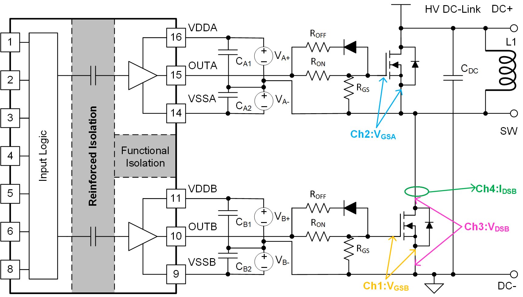
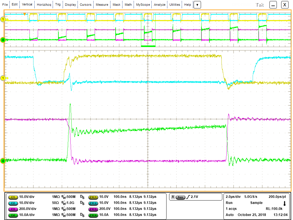
Figure 8-5 shows a multiple pulses bench test circuit which uses L1 as the inductor load, and a group of control pulses are generated to evaluate driver and SiC MOSFET switching transient under different load conditions. The test conditions are: VDC-Link = 600 V, VCC = 5 V, VDD = 15 V, VSS = –4 V, fSW = 500 kHz, RON = 5.1 Ω, ROFF = 1.0 Ω. Figure 8-6 shows the turn on and turn off waveforms at around 20 A current
Channel 1 (Yellow): Gate-source voltage signal on the low side MOSFET.
Channel 2 (Blue): Gate-source voltage signal on the high side MOSFET.
Channel 3 (Pink): Drain-source voltage signal for the low side MOSFET.
Channel 4 (Green): Drain-source current signal for the low side MOSFET.
In Figure 8-6, the gate drive signals on the high and low power transistor have a 100-ns dead time, and both signals are measured with >= 500 MHz bandwidth probes.
 Figure 8-5 Bench
Test Circuit with SiC MOSFET Switching
 Figure 8-6 SiC
MOSFET Switching Waveforms