SLUSDG3E August 2018 – August 2024 UCC21530-Q1
PRODUCTION DATA
- 1
- 1 Features
- 2 Applications
- 3 Description
- 4 Pin Configuration and Functions
-
5 Specifications
- 5.1 Absolute Maximum Ratings
- 5.2 ESD Ratings (Automotive)
- 5.3 Recommended Operating Conditions
- 5.4 Thermal Information
- 5.5 Power Ratings
- 5.6 Insulation Specifications
- 5.7 Safety Limiting Values
- 5.8 Electrical Characteristics
- 5.9 Timing Requirements
- 5.10 Switching Characteristics
- 5.11 Insulation Characteristics Curves
- 5.12 Typical Characteristics
- 6 Parameter Measurement Information
- 7 Detailed Description
-
8 Application and Implementation
- 8.1 Application Information
- 8.2
Typical Application
- 8.2.1 Design Requirements
- 8.2.2 Detailed Design Procedure
- 8.2.3 Application Curves
- 9 Power Supply Recommendations
- 10Layout
- 11Device and Documentation Support
- 12Revision History
- 13Mechanical, Packaging, and Orderable Information
Package Options
Refer to the PDF data sheet for device specific package drawings
Mechanical Data (Package|Pins)
- DWK|14
Thermal pad, mechanical data (Package|Pins)
Orderable Information
8.2.2.5 Estimating Junction Temperature
The junction temperature of the UCC21530-Q1 can be estimated with:
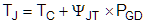
where
- TJ is the junction temperature.
- TC is the UCC21530-Q1 case-top temperature measured with a thermocouple or some other instrument.
- ψJT is the junction-to-top characterization parameter from the Thermal Information table.
Using the junction-to-top characterization parameter (ΨJT) instead of the junction-to-case thermal resistance (RΘJC) can greatly improve the accuracy of the junction temperature estimation. The majority of the thermal energy of most ICs is released into the PCB through the package leads, whereas only a small percentage of the total energy is released through the top of the case (where thermocouple measurements are usually conducted). RΘJC can only be used effectively when most of the thermal energy is released through the case, such as with metal packages or when a heatsink is applied to an IC package. In all other cases, use of RΘJC will inaccurately estimate the true junction temperature. ΨJT is experimentally derived by assuming that the amount of energy leaving through the top of the IC will be similar in both the testing environment and the application environment. As long as the recommended layout guidelines are observed, junction temperature estimates can be made accurately to within a few degrees Celsius. For more information, see the Section 10.1 and Semiconductor and IC Package Thermal Metrics Application Report.