SLUSEW9D May 2023 – June 2024 UCC21551
PRODUCTION DATA
- 1
- 1 Features
- 2 Applications
- 3 Description
- 4 Pin Configuration and Functions
-
5 Specifications
- 5.1 Absolute Maximum Ratings
- 5.2 ESD Ratings
- 5.3 Recommended Operating Conditions
- 5.4 Thermal Information
- 5.5 Power Ratings
- 5.6 Insulation Specifications
- 5.7 Safety Limiting Values
- 5.8 Electrical Characteristics
- 5.9 Switching Characteristics
- 5.10 Insulation Characteristics Curves
- 5.11 Typical Characteristics
- 6 Parameter Measurement Information
- 7 Detailed Description
-
8 Application and Implementation
- 8.1 Application Information
- 8.2
Typical Application
- 8.2.1 Design Requirements
- 8.2.2
Detailed Design Procedure
- 8.2.2.1 Designing INA/INB Input Filter
- 8.2.2.2 Select External Bootstrap Diode and its Series Resistor
- 8.2.2.3 Gate Driver Output Resistor
- 8.2.2.4 Gate to Source Resistor Selection
- 8.2.2.5 Estimate Gate Driver Power Loss
- 8.2.2.6 Estimating Junction Temperature
- 8.2.2.7 Selecting VCCI, VDDA/B Capacitor
- 8.2.2.8 Dead Time Setting Guidelines
- 8.2.2.9 Application Circuits with Output Stage Negative Bias
- 8.2.3 Application Curves
- 9 Power Supply Recommendations
- 10Layout
- 11Device and Documentation Support
- 12Revision History
- 13Mechanical, Packaging, and Orderable Information
Package Options
Refer to the PDF data sheet for device specific package drawings
Mechanical Data (Package|Pins)
- DWK|14
- DW|16
Thermal pad, mechanical data (Package|Pins)
- DW|16
Orderable Information
13.1 Tape and Reel Information
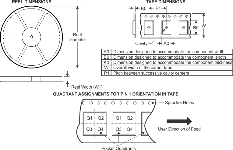
| Device | Package Type |
Package Drawing | Pins | SPQ | Reel Diameter (mm) |
Reel Width W1 (mm) |
A0 (mm) |
B0 (mm) |
K0 (mm) |
P1 (mm) |
W (mm) |
Pin1 Quadrant |
|---|---|---|---|---|---|---|---|---|---|---|---|---|
| UCC21551ADWKR | SOIC | DWK | 14 | 2000 | 330 | 16.4 | 10.75 | 10.7 | 2.7 | 12 | 16 | Q1 |
| UCC21551ADWR | SOIC | DW | 16 | 2000 | 330 | 16.4 | 10.75 | 10.7 | 2.7 | 12 | 16 | Q1 |
| UCC21551BDWKR | SOIC | DWK | 14 | 2000 | 330 | 16.4 | 10.75 | 10.7 | 2.7 | 12 | 16 | Q1 |
| UCC21551CDWKR | SOIC | DWK | 14 | 2000 | 330 | 16.4 | 10.75 | 10.7 | 2.7 | 12 | 16 | Q1 |
| UCC21551DDWKR | SOIC | DWK | 14 | 2000 | 330 | 16.4 | 10.75 | 10.7 | 2.7 | 12 | 16 | Q1 |
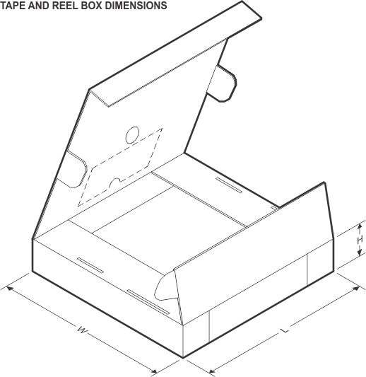
| Device | Package Type | Package Drawing | Pins | SPQ | Length (mm) | Width (mm) | Height (mm) |
|---|---|---|---|---|---|---|---|
| UCC21551ADWKR | SOIC | DWK | 14 | 2000 | 353 | 353 | 32 |
| UCC21551ADWR | SOIC | DW | 16 | 2000 | 353 | 353 | 32 |
| UCC21551BDWKR | SOIC | DWK | 14 | 2000 | 356 | 356 | 35 |
| UCC21551CDWKR | SOIC | DWK | 14 | 2000 | 356 | 356 | 35 |
| UCC21551DDWKR | SOIC | DWK | 14 | 2000 | 356 | 356 | 35 |