SLUSEK4B April 2022 – June 2024 UCC21717-Q1
PRODUCTION DATA
- 1
- 1 Features
- 2 Applications
- 3 Description
- 4 Pin Configuration and Functions
-
5 Specifications
- 5.1 Absolute Maximum Ratings
- 5.2 ESD Ratings
- 5.3 Recommended Operating Conditions
- 5.4 Thermal Information
- 5.5 Power Ratings
- 5.6 Insulation Specifications
- 5.7 Safety Limiting Values
- 5.8 Electrical Characteristics
- 5.9 Switching Characteristics
- 5.10 Insulation Characteristics Curves
- 5.11 Typical Characteristics
- 6 Parameter Measurement Information
-
7 Detailed Description
- 7.1 Overview
- 7.2 Functional Block Diagram
- 7.3
Feature Description
- 7.3.1 Power Supply
- 7.3.2 Driver Stage
- 7.3.3 VCC and VDD Undervoltage Lockout (UVLO)
- 7.3.4 Active Pulldown
- 7.3.5 Short Circuit Clamping
- 7.3.6 Internal Active Miller Clamp
- 7.3.7 Overcurrent and Short Circuit Protection
- 7.3.8 Soft Turn-Off
- 7.3.9 Fault (FLT), Reset and Enable (RST/EN)
- 7.3.10 Isolated Analog to PWM Signal Function
- 7.4 Device Functional Modes
-
8 Applications and Implementation
- 8.1 Application Information
- 8.2
Typical Application
- 8.2.1 Design Requirements
- 8.2.2
Detailed Design Procedure
- 8.2.2.1 Input Filters for IN+, IN-, and RST/EN
- 8.2.2.2 PWM Interlock of IN+ and IN-
- 8.2.2.3 FLT, RDY, and RST/EN Pin Circuitry
- 8.2.2.4 RST/EN Pin Control
- 8.2.2.5 Turn-On and Turn-Off Gate Resistors
- 8.2.2.6 Overcurrent and Short Circuit Protection
- 8.2.2.7 Isolated Analog Signal Sensing
- 8.2.2.8 Higher Output Current Using an External Current Buffer
- 9 Power Supply Recommendations
- 10Layout
- 11Device and Documentation Support
- 12Revision History
- 13Mechanical, Packaging, and Orderable Information
Package Options
Mechanical Data (Package|Pins)
- DW|16
Thermal pad, mechanical data (Package|Pins)
- DW|16
Orderable Information
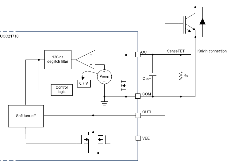
7.3.8 Soft Turn-Off
The UCC21717-Q1 initiates a soft turn-off when the overcurrent and short circuit protection are triggered, or when the RST/EN is pulled low for longer than tRSTPD. When the overcurrent and short circuit faults occur, the power semiconductor transitions from the linear region to the saturation region very quickly. The gate voltage controls the channel current. By pulling down the gate voltage with a soft turn-off current, the dI/dt of the channel current is controlled by the gate voltage and decreases softly; thus, overshooting the power semiconductor is limited, preventing overvoltage breakdown. Figure 6-10 shows the the soft turn-off timing diagram.
 Figure 7-6 Soft Turn-Off