SLUSDS3A March 2020 – January 2024 UCC21739-Q1
PRODUCTION DATA
- 1
- 1 Features
- 2 Applications
- 3 Description
- 4 Pin Configuration and Functions
-
5 Specifications
- 5.1 Absolute Maximum Ratings
- 5.2 ESD Ratings
- 5.3 Recommended Operating Conditions
- 5.4 Thermal Information
- 5.5 Power Ratings
- 5.6 Insulation Specifications
- 5.7 Safety-Related Certifications
- 5.8 Safety Limiting Values
- 5.9 Electrical Characteristics
- 5.10 Switching Characteristics
- 5.11 Insulation Characteristics Curves
- 5.12 Typical Characteristics
- 6 Parameter Measurement Information
-
7 Detailed Description
- 7.1 Overview
- 7.2 Functional Block Diagram
- 7.3
Feature Description
- 7.3.1 Power Supply
- 7.3.2 Driver Stage
- 7.3.3 VCC and VDD Undervoltage Lockout (UVLO)
- 7.3.4 Active Pulldown
- 7.3.5 Short Circuit Clamping
- 7.3.6 External Active Miller Clamp
- 7.3.7 Overcurrent and Short Circuit Protection
- 7.3.8 2-Level Turn-off
- 7.3.9 Fault ( FLT, Reset and Enable ( RST/EN)
- 7.3.10 Isolated Analog to PWM Signal Function
- 7.4 Device Functional Modes
-
8 Applications and Implementation
- 8.1 Application Information
- 8.2
Typical Application
- 8.2.1 Design Requirements
- 8.2.2
Detailed Design Procedure
- 8.2.2.1 Input filters for IN+, IN- and RST/EN
- 8.2.2.2 PWM Interlock of IN+ and IN-
- 8.2.2.3 FLT, RDY and RST/EN Pin Circuitry
- 8.2.2.4 RST/EN Pin Control
- 8.2.2.5 Turn-On and Turn-Off Gate Resistors
- 8.2.2.6 External Active Miller Clamp
- 8.2.2.7 Overcurrent and Short Circuit Protection
- 8.2.2.8 Isolated Analog Signal Sensing
- 8.2.2.9 Higher Output Current Using an External Current Buffer
- 8.2.3 Application Curves
- 9 Power Supply Recommendations
- 10Layout
- 11Device and Documentation Support
- 12Revision History
- 13Mechanical, Packaging, and Orderable Information
Package Options
Mechanical Data (Package|Pins)
- DW|16
Thermal pad, mechanical data (Package|Pins)
- DW|16
Orderable Information
8.2.2.4 RST/EN Pin Control
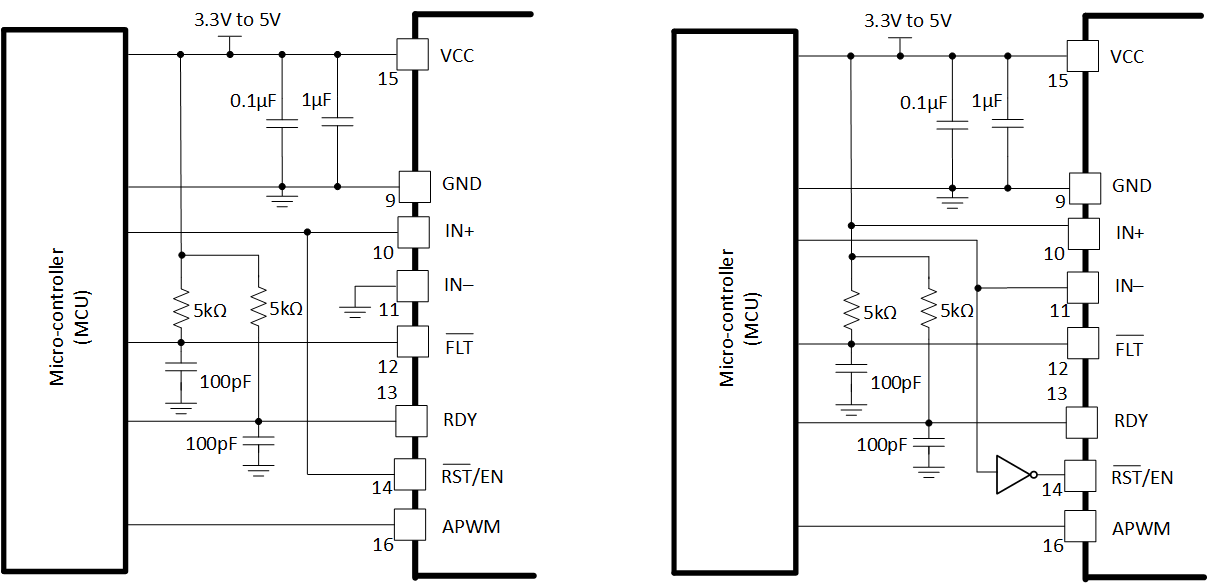
RST/EN pin has two functions. It can be used to enable and shutdown the outputs of the driver, and reset the fault signaled on the FLT pin. RST/EN pin needs to be pulled up to enable the device; when the pin is pulled down, the device is in disabled status. With a 50kΩ pulldown resistor existing, the driver is disabled by default.
When the driver is latched after overcurrent or short circuit fault is detected, the FLT pin and output are latched low and need to be reset by RST/EN pin. RST/EN pin is active low. The microcntroller needs to send a signal to RST/EN pin after the fault mute time tFLTMUTE to reset the driver. This pin can also be used to automatically reset the driver. The continuous input signal IN+ or IN- can be applied to RST/EN pin, so the microcontroller does not need to generate another control signal to reset the driver. If non-inverting input IN+ is used, then IN+ can be tied to RST/EN pin. If inverting input IN- is used, then a NOT logic is needed between the inverting PWM signal from the microcontroller and the RST/EN pin. In this case, the driver can be reset in every switching cycle without an extra control signal from microcontroller to RST/EN pin.
 Figure 8-4 Automatic Reset Control