SLUSEM9A September 2022 – June 2024 UCC21755-Q1
PRODUCTION DATA
- 1
- 1 Features
- 2 Applications
- 3 Description
- 4 Pin Configuration and Functions
-
5 Specifications
- 5.1 Absolute Maximum Ratings
- 5.2 ESD Ratings
- 5.3 Recommended Operating Conditions
- 5.4 Thermal Information
- 5.5 Power Ratings
- 5.6 Insulation Specifications
- 5.7 Safety Limiting Values
- 5.8 Electrical Characteristics
- 5.9 Switching Characteristics
- 5.10 Insulation Characteristics Curves
- 5.11 Typical Characteristics
- 6 Parameter Measurement Information
-
7 Detailed Description
- 7.1 Overview
- 7.2 Functional Block Diagram
- 7.3
Feature Description
- 7.3.1 Power Supply
- 7.3.2 Driver Stage
- 7.3.3 VCC and VDD Undervoltage Lockout (UVLO)
- 7.3.4 Active Pulldown
- 7.3.5 Short Circuit Clamping
- 7.3.6 Internal Active Miller Clamp
- 7.3.7 Desaturation (DESAT) Protection
- 7.3.8 Soft Turn-Off
- 7.3.9 Fault (FLT), Reset and Enable (RST/EN)
- 7.3.10 Isolated Analog to PWM Signal Function
- 7.4 Device Functional Modes
-
8 Applications and Implementation
- 8.1 Application Information
- 8.2
Typical Application
- 8.2.1 Design Requirements
- 8.2.2
Detailed Design Procedure
- 8.2.2.1 Input Filters for IN+, IN-, and RST/EN
- 8.2.2.2 PWM Interlock of IN+ and IN-
- 8.2.2.3 FLT, RDY, and RST/EN Pin Circuitry
- 8.2.2.4 RST/EN Pin Control
- 8.2.2.5 Turn-On and Turn-Off Gate Resistors
- 8.2.2.6 Overcurrent and Short Circuit Protection
- 8.2.2.7 Isolated Analog Signal Sensing
- 8.2.2.8 Higher Output Current Using an External Current Buffer
- 8.2.3 Application Curves
- 9 Power Supply Recommendations
- 10Layout
- 11Device and Documentation Support
- 12Revision History
- 13Mechanical, Packaging, and Orderable Information
Package Options
Mechanical Data (Package|Pins)
- DW|16
Thermal pad, mechanical data (Package|Pins)
- DW|16
Orderable Information
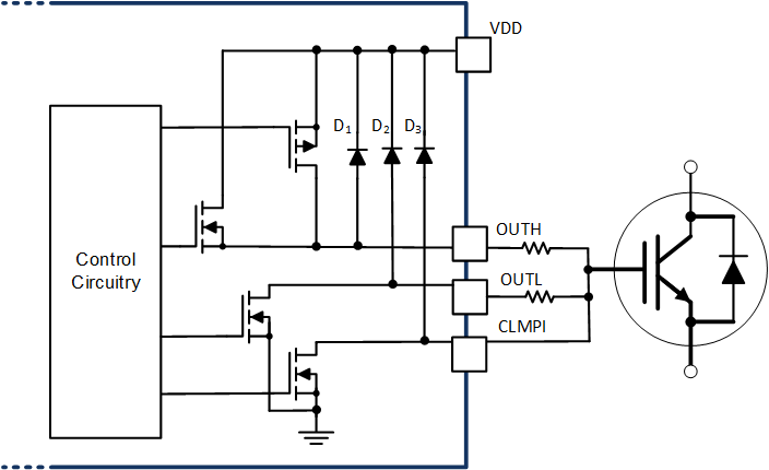
7.3.5 Short Circuit Clamping
During short circuit condition, the Miller capacitance can cause a current sinking to the OUTH/OUTL/CLMPI pin due to the high dV/dt and boost the OUTH/OUTL/CLMPI voltage. The short circuit clamping feature of the device can clamp the OUTH/OUTL/CLMPI pin voltage to be slightly higher than VDD, which can protect the power semiconductors from a gate-source and gate-emitter overvoltage breakdown. This feature is realized by an internal diode from the OUTH/OUTL/CLMPI to VDD.
 Figure 7-3 Short Circuit Clamping