SLUSEM9A September 2022 – June 2024 UCC21755-Q1
PRODUCTION DATA
- 1
- 1 Features
- 2 Applications
- 3 Description
- 4 Pin Configuration and Functions
-
5 Specifications
- 5.1 Absolute Maximum Ratings
- 5.2 ESD Ratings
- 5.3 Recommended Operating Conditions
- 5.4 Thermal Information
- 5.5 Power Ratings
- 5.6 Insulation Specifications
- 5.7 Safety Limiting Values
- 5.8 Electrical Characteristics
- 5.9 Switching Characteristics
- 5.10 Insulation Characteristics Curves
- 5.11 Typical Characteristics
- 6 Parameter Measurement Information
-
7 Detailed Description
- 7.1 Overview
- 7.2 Functional Block Diagram
- 7.3
Feature Description
- 7.3.1 Power Supply
- 7.3.2 Driver Stage
- 7.3.3 VCC and VDD Undervoltage Lockout (UVLO)
- 7.3.4 Active Pulldown
- 7.3.5 Short Circuit Clamping
- 7.3.6 Internal Active Miller Clamp
- 7.3.7 Desaturation (DESAT) Protection
- 7.3.8 Soft Turn-Off
- 7.3.9 Fault (FLT), Reset and Enable (RST/EN)
- 7.3.10 Isolated Analog to PWM Signal Function
- 7.4 Device Functional Modes
-
8 Applications and Implementation
- 8.1 Application Information
- 8.2
Typical Application
- 8.2.1 Design Requirements
- 8.2.2
Detailed Design Procedure
- 8.2.2.1 Input Filters for IN+, IN-, and RST/EN
- 8.2.2.2 PWM Interlock of IN+ and IN-
- 8.2.2.3 FLT, RDY, and RST/EN Pin Circuitry
- 8.2.2.4 RST/EN Pin Control
- 8.2.2.5 Turn-On and Turn-Off Gate Resistors
- 8.2.2.6 Overcurrent and Short Circuit Protection
- 8.2.2.7 Isolated Analog Signal Sensing
- 8.2.2.8 Higher Output Current Using an External Current Buffer
- 8.2.3 Application Curves
- 9 Power Supply Recommendations
- 10Layout
- 11Device and Documentation Support
- 12Revision History
- 13Mechanical, Packaging, and Orderable Information
Package Options
Mechanical Data (Package|Pins)
- DW|16
Thermal pad, mechanical data (Package|Pins)
- DW|16
Orderable Information
8.2.2.7.1 Isolated Temperature Sensing
A typical application circuit is shown in Figure 6-8. To sense temperature, the AIN pin is connected to the thermal diode or thermistor which can be discrete or integrated within the power module. A low-pass filter is recommended for the AIN input. Since the temperature signal does not have a high bandwidth, the low-pass filter is mainly used for filtering the noise introduced by the switching of the power device, which does not require stringent control for propagation delay. The filter capacitance for Cfilt can be chosen between 1 nF to 100 nF and the filter resistance Rfilt between 1 Ω to 10 Ω according to the noise level.
The output of APWM is directly connected to the microcontroller to measure the duty cycle dependent on the voltage input at AIN, using Equation 9.
 Figure 8-7 Thermal Diode or Thermistor Temperature Sensing Configuration
When a high-precision voltage supply for VCC is used on the primary side of the device, the duty cycle output of APWM may also be filtered and the voltage measured using the microcontroller's ADC input pin, as shown in Figure 8-8. The frequency of APWM is 400 kHz, so the value for Rfilt_2 and Cfilt_2 should be such that the cutoff frequency is below 400 kHz. Temperature does not change rapidly, thus the rise time due to the RC constant of the filter is not under a strict requirement.
 Figure 8-8 APWM Channel with Filtered Output
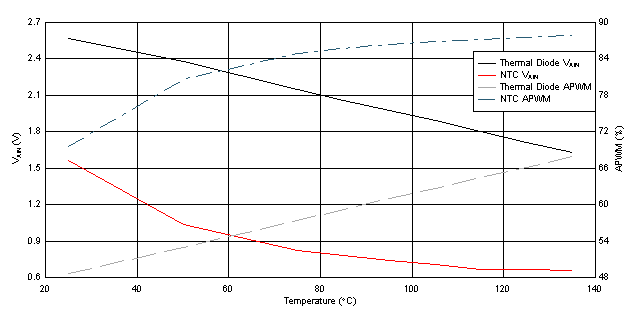
The example below shows the results using a 4.7-kΩ NTC, NTCS0805E3472FMT, in series with a 3-kΩ resistor and also the thermal diode using four diode-connected MMBT3904 NPN transistors. The sensed voltage of the 4 MMBT3904 thermal diodes connected in series ranges from about 2.5 V to 1.6 V from 25°C to 135°C, corresponding to 50% to 68% duty cycle. The sensed voltage of the NTC thermistor connected in series with the 3-kΩ resistor ranges from about 1.5 V to 0.6 V from 25°C to 135°C, corresponding to 70% to 88% duty cycle. The voltage at VAIN of both sensors and the corresponding measured duty cycle at APWM is shown in Figure 8-9.
 Figure 8-9 Thermal Diode and NTC VAIN and
Corresponding Duty Cycle at APWM
Figure 8-9 Thermal Diode and NTC VAIN and
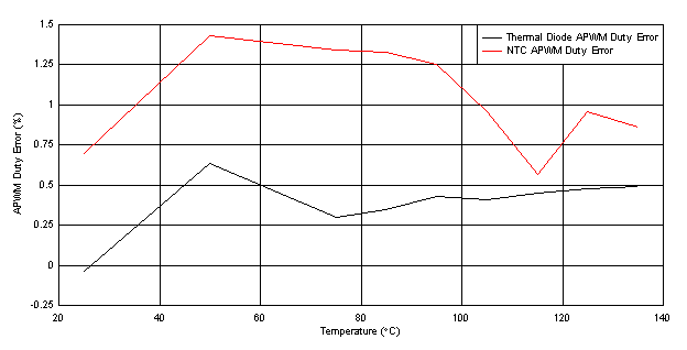
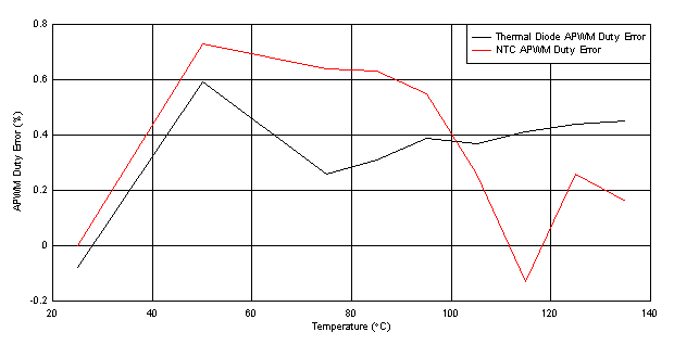
Corresponding Duty Cycle at APWMThe duty cycle output has an accuracy of ±3% throughout temperature without any calibration, as shown in Figure 8-10 but with single-point calibration at 25°C, the duty accuracy can be improved to ±1%, as shown in Figure 8-11.
 Figure 8-10 APWM Duty Error Without Calibration
 Figure 8-11 APWM Duty Error with Single-Point Calibration