SLUSEM9A September 2022 – June 2024 UCC21755-Q1
PRODUCTION DATA
- 1
- 1 Features
- 2 Applications
- 3 Description
- 4 Pin Configuration and Functions
-
5 Specifications
- 5.1 Absolute Maximum Ratings
- 5.2 ESD Ratings
- 5.3 Recommended Operating Conditions
- 5.4 Thermal Information
- 5.5 Power Ratings
- 5.6 Insulation Specifications
- 5.7 Safety Limiting Values
- 5.8 Electrical Characteristics
- 5.9 Switching Characteristics
- 5.10 Insulation Characteristics Curves
- 5.11 Typical Characteristics
- 6 Parameter Measurement Information
-
7 Detailed Description
- 7.1 Overview
- 7.2 Functional Block Diagram
- 7.3
Feature Description
- 7.3.1 Power Supply
- 7.3.2 Driver Stage
- 7.3.3 VCC and VDD Undervoltage Lockout (UVLO)
- 7.3.4 Active Pulldown
- 7.3.5 Short Circuit Clamping
- 7.3.6 Internal Active Miller Clamp
- 7.3.7 Desaturation (DESAT) Protection
- 7.3.8 Soft Turn-Off
- 7.3.9 Fault (FLT), Reset and Enable (RST/EN)
- 7.3.10 Isolated Analog to PWM Signal Function
- 7.4 Device Functional Modes
-
8 Applications and Implementation
- 8.1 Application Information
- 8.2
Typical Application
- 8.2.1 Design Requirements
- 8.2.2
Detailed Design Procedure
- 8.2.2.1 Input Filters for IN+, IN-, and RST/EN
- 8.2.2.2 PWM Interlock of IN+ and IN-
- 8.2.2.3 FLT, RDY, and RST/EN Pin Circuitry
- 8.2.2.4 RST/EN Pin Control
- 8.2.2.5 Turn-On and Turn-Off Gate Resistors
- 8.2.2.6 Overcurrent and Short Circuit Protection
- 8.2.2.7 Isolated Analog Signal Sensing
- 8.2.2.8 Higher Output Current Using an External Current Buffer
- 8.2.3 Application Curves
- 9 Power Supply Recommendations
- 10Layout
- 11Device and Documentation Support
- 12Revision History
- 13Mechanical, Packaging, and Orderable Information
Package Options
Mechanical Data (Package|Pins)
- DW|16
Thermal pad, mechanical data (Package|Pins)
- DW|16
Orderable Information
7.3.8 Soft Turn-Off
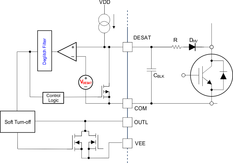
The device initiates a soft turn-off when the overcurrent and short circuit protection are triggered. When the overcurrent and short circuit faults occur, the IGBT transits from the active region to the desaturation region very quickly. The channel current is controlled by the gate voltage and decreases softly; thus, the overshoot of the IGBT is limited and prevents the overvoltage breakdown. There is a tradeoff between the overshoot voltage and short circuit energy. The turn-off speed should be slow to limit the overshoot-voltage, but the shutdown time should not be too long that the large energy dissipation can breakdown the device. The 400-mA soft turn-off current of the device ensures the power switches are safely turned off during short circuit events. Figure 6-10 shows the soft turn-off timing diagram.
 Figure 7-6 Soft Turn-Off