SLUS846D September 2008 – August 2024 UCC25600
PRODUCTION DATA
- 1
- 1 Features
- 2 Applications
- 3 Description
- 4 Revision History
- 5 Pin Configuration and Functions
- 6 Specifications
- 7 Detailed Description
- 8 Application and Implementation
- 9 Power Supply Recommendations
- 10Layout
- 11Device and Documentation Support
- 12Glossary
- 13Mechanical, Packaging, and Orderable Information
Package Options
Mechanical Data (Package|Pins)
- D|8
Thermal pad, mechanical data (Package|Pins)
Orderable Information
8.2.2 Detailed Design Procedure
- Resonant inductor (Lr), resonant capacitor (Cr), and Lm of half-bridge LLC
- Turns ratio of Main transformer:
Equation 23. n = Np/Ns = 16.5
- Maximum resonant gain required:
Equation 24. M_max = 110% × n × (2 × Vout)/(Vin_min) = 110% × 16.5 × (2 × 12 V)/375 V = 1.17
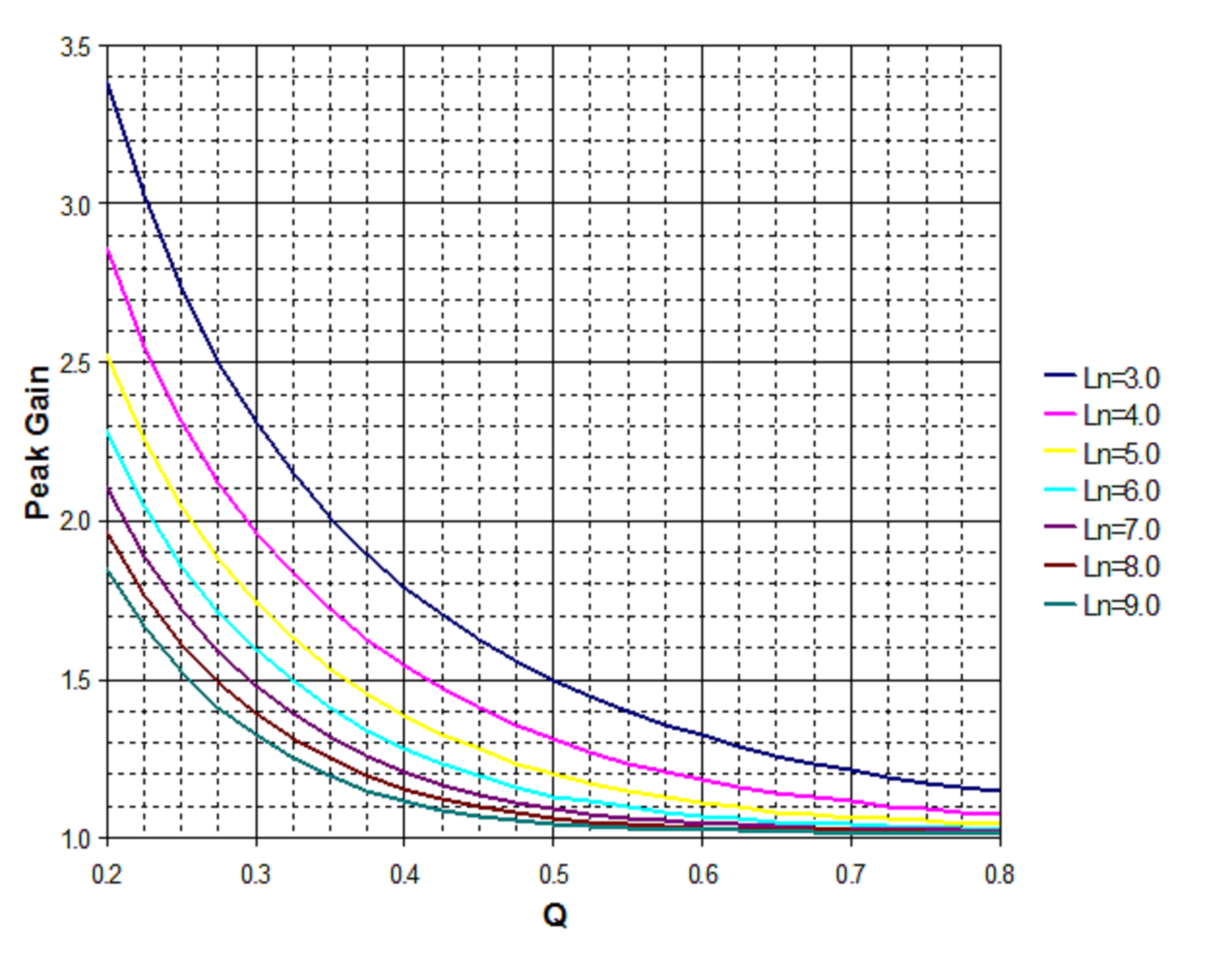
- Choose Ln and Q. The Ln range is typically selected from 3 to 9. Choose Q based on the curves below, where the peak gain must be higher than or equal to the maximum resonant gain required. Based on the below curves, Q selects 0.45.
Equation 25. Ln = Lm/Lr = 5Equation 26.

 Figure 8-9 Peak Gain vs Q
 - Calculate equivalent primary resistance:
Equation 27. Req = (8 × n2 × Vout2)/(π2 × Pout) = (8 × 4.62 × 122)/(π2 × 300) = 108.6Ω
- Select Cr:
Equation 28. Cr = 24nF
- Calculate Lr:
Equation 29.

- Combine the above two equations:
Equation 30. Lr = 55 µH
- Calculate Lm:
Equation 31. Lm = Ln × Lr = 275 µH
- Turns ratio of Main transformer:
- Calculate Rdt. In the UCC25600, dead time can be adjusted through a single resistor from DT pin to ground. With an internal 2.25-V voltage reference, the current flow through the resistor sets the dead time.
Equation 32. td = 20ns + Rdt × 24ns/kΩ
where
- td = 300 ns
- Rdt = 11.7 kΩ
- Calculate CSS. Refer to Soft Start for more details.
Equation 33. tss = 25 msEquation 34. tss = 2.8 V/5 µA × CssEquation 35. Css = 44.6 nF
- A 47nF capacitor is selected. Calculate RT1 and RT2. Refer to Oscillator for more details. RT1 and RT2 are used to limit maximum switching frequency and minimum switching frequency. RT1 and RT2 can be calculated based on following equations:
Equation 36. Ifmax = 6 ns/(1/2fmax - 150 ns)Equation 37. Ifmin = 6 ns/(1/2fmin - 150 ns)Equation 38. Ifmax = 2.5 V(1/RT1 + 1/RT2)Equation 39. Ifmin = 2.5 V/RT2
- Combine the four equations above:
Equation 40. RT1 = 511ΩEquation 41. RT2 = 2.37 kΩ
- Calculate Rs, Cs, Rp, and Cp. Refer to Overcurrent Protection for more details.
Equation 42. Rs = 300 kΩEquation 43. Cs = 22 pFEquation 44. Rp = 4.99 kΩEquation 45. Cp = 1 µF