SLUS846D September 2008 – August 2024 UCC25600
PRODUCTION DATA
- 1
- 1 Features
- 2 Applications
- 3 Description
- 4 Revision History
- 5 Pin Configuration and Functions
- 6 Specifications
- 7 Detailed Description
- 8 Application and Implementation
- 9 Power Supply Recommendations
- 10Layout
- 11Device and Documentation Support
- 12Glossary
- 13Mechanical, Packaging, and Orderable Information
Package Options
Mechanical Data (Package|Pins)
- D|8
Thermal pad, mechanical data (Package|Pins)
Orderable Information
8.2.3 Application Curves
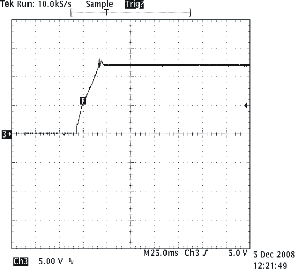
 Figure 8-10 Typical Output Voltage Turn On (TP15)
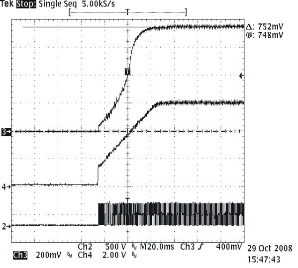
 Figure 8-12 Typical Soft-Start Waveform
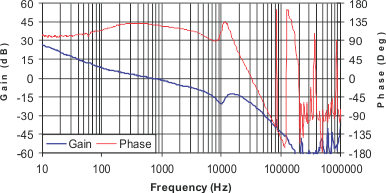
 Figure 8-11 Full System Loop Compensation (TP19 and TP21)
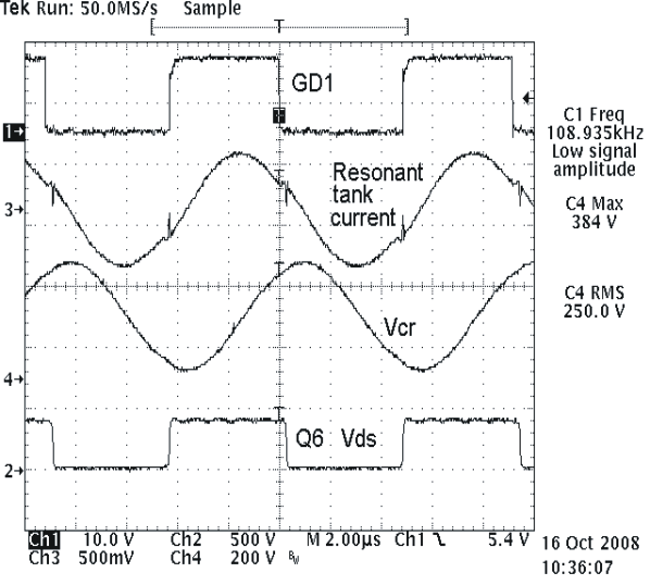
 Figure 8-13 Typical Resonant Tank Current and Resonant Capacitor Voltage