SLUSCU6C August 2017 – January 2020 UCC256301
PRODUCTION DATA.
- 1 Features
- 2 Applications
- 3 Description
- 4 Revision History
- 5 Pin Configuration and Functions
- 6 Specifications
-
7 Detailed Description
- 7.1 Overview
- 7.2 Functional Block Diagram
- 7.3
Feature Description
- 7.3.1 Hybrid Hysteretic Control
- 7.3.2 Regulated 12-V Supply
- 7.3.3 Feedback Chain
- 7.3.4 Optocoupler Feedback Signal Input and Bias
- 7.3.5 System External Shut Down
- 7.3.6 Pick Lower Block and Soft Start Multiplexer
- 7.3.7 Pick Higher Block and Burst Mode Multiplexer
- 7.3.8 VCR Comparators
- 7.3.9 Resonant Capacitor Voltage Sensing
- 7.3.10 Resonant Current Sensing
- 7.3.11 Bulk Voltage Sensing
- 7.3.12 Output Voltage Sensing
- 7.3.13 High Voltage Gate Driver
- 7.3.14 Protections
- 7.4 Device Functional Modes
-
8 Application and Implementation
- 8.1 Application Information
- 8.2
Typical Application
- 8.2.1 Design Requirements
- 8.2.2
Detailed Design Procedure
- 8.2.2.1 LLC Power Stage Requirements
- 8.2.2.2 LLC Gain Range
- 8.2.2.3 Select Ln and Qe
- 8.2.2.4 Determine Equivalent Load Resistance
- 8.2.2.5 Determine Component Parameters for LLC Resonant Circuit
- 8.2.2.6 LLC Primary-Side Currents
- 8.2.2.7 LLC Secondary-Side Currents
- 8.2.2.8 LLC Transformer
- 8.2.2.9 LLC Resonant Inductor
- 8.2.2.10 LLC Resonant Capacitor
- 8.2.2.11 LLC Primary-Side MOSFETs
- 8.2.2.12 Design Considerations for Adaptive Dead-Time
- 8.2.2.13 LLC Rectifier Diodes
- 8.2.2.14 LLC Output Capacitors
- 8.2.2.15 HV Pin Series Resistors
- 8.2.2.16 BLK Pin Voltage Divider
- 8.2.2.17 BW Pin Voltage Divider
- 8.2.2.18 ISNS Pin Differentiator
- 8.2.2.19 VCR Pin Capacitor Divider
- 8.2.2.20 Burst Mode Programming
- 8.2.2.21 Soft-Start Capacitor
- 8.2.3 Application Curves
- 9 Power Supply Recommendations
- 10Layout
- 11Device and Documentation Support
- 12Mechanical, Packaging, and Orderable Information
Package Options
Mechanical Data (Package|Pins)
- DDB|14
Thermal pad, mechanical data (Package|Pins)
Orderable Information
7.3.12 Output Voltage Sensing
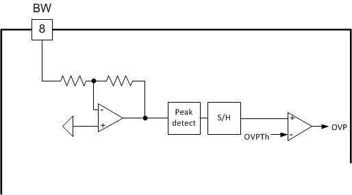
The output voltage is sensed through the bias winding (BW) voltage sense pin. The sensed output voltage is compared with a fixed threshold to generate output OVP fault. The block diagram of the bias winding voltage sense block is shown below.
 Figure 38. Bias Winding Sensing Block Diagram
 The bias winding sense block consists of an inverting op amp to flip the BW signal. The flipped BW signal is then peak detected and sampled at low side turn off edge. The sampled voltage represents the output voltage during this cycle. The S/H output is them compared with OVP comparator. Shown below is the timing diagram of the BW sense block.
 Figure 39. Timing Diagram of BW Sense Block