SLUSD49A September   2017  – January 2019 UCC256303

PRODUCTION DATA.  

  1. Features
  2. Applications
  3. Description
    1.     Simplified Schematic
  4. Revision History
  5. Pin Configuration and Functions
    1.     Pin Functions
  6. Specifications
    1. 6.1 Absolute Maximum Ratings
    2. 6.2 ESD Ratings
    3. 6.3 Recommended Operating Conditions
    4. 6.4 Thermal Information
    5. 6.5 Electrical Characteristics
    6. 6.6 Switching Characteristics
    7. 6.7 Typical Characteristics
  7. Detailed Description
    1. 7.1 Overview
    2. 7.2 Functional Block Diagram
    3. 7.3 Feature Description
      1. 7.3.1  Hybrid Hysteretic Control
      2. 7.3.2  Regulated 12-V Supply
      3. 7.3.3  Feedback Chain
      4. 7.3.4  Optocoupler Feedback Signal Input and Bias
      5. 7.3.5  System External Shut Down
      6. 7.3.6  Pick Lower Block and Soft Start Multiplexer
      7. 7.3.7  Pick Higher Block and Burst Mode Multiplexer
      8. 7.3.8  VCR Comparators
      9. 7.3.9  Resonant Capacitor Voltage Sensing
      10. 7.3.10 Resonant Current Sensing
      11. 7.3.11 Bulk Voltage Sensing
      12. 7.3.12 Output Voltage Sensing
      13. 7.3.13 High Voltage Gate Driver
      14. 7.3.14 Protections
        1. 7.3.14.1 ZCS Region Prevention
        2. 7.3.14.2 Over Current Protection (OCP)
        3. 7.3.14.3 Over Output Voltage Protection (VOUTOVP)
        4. 7.3.14.4 Over Input Voltage Protection (VINOVP)
        5. 7.3.14.5 Under Input Voltage Protection (VINUVP)
        6. 7.3.14.6 Boot UVLO
        7. 7.3.14.7 RVCC UVLO
        8. 7.3.14.8 Over Temperature Protection (OTP)
    4. 7.4 Device Functional Modes
      1. 7.4.1 Burst Mode Control
      2. 7.4.2 Soft-Start and Burst-Mode Threshold
      3. 7.4.3 System States and Faults State Machine
      4. 7.4.4 Waveform Generator State Machine
  8. Application and Implementation
    1. 8.1 Application Information
    2. 8.2 Typical Application
      1. 8.2.1 Design Requirements
      2. 8.2.2 Detailed Design Procedure
        1. 8.2.2.1  LLC Power Stage Requirements
        2. 8.2.2.2  LLC Gain Range
        3. 8.2.2.3  Select Ln and Qe
        4. 8.2.2.4  Determine Equivalent Load Resistance
        5. 8.2.2.5  Determine Component Parameters for LLC Resonant Circuit
        6. 8.2.2.6  LLC Primary-Side Currents
        7. 8.2.2.7  LLC Secondary-Side Currents
        8. 8.2.2.8  LLC Transformer
        9. 8.2.2.9  LLC Resonant Inductor
        10. 8.2.2.10 LLC Resonant Capacitor
        11. 8.2.2.11 LLC Primary-Side MOSFETs
        12. 8.2.2.12 Design Considerations for Adaptive Dead-Time
        13. 8.2.2.13 LLC Rectifier Diodes
        14. 8.2.2.14 LLC Output Capacitors
        15. 8.2.2.15 BLK Pin Voltage Divider
        16. 8.2.2.16 BW Pin Voltage Divider
        17. 8.2.2.17 ISNS Pin Differentiator
        18. 8.2.2.18 VCR Pin Capacitor Divider
        19. 8.2.2.19 Burst Mode Programming
        20. 8.2.2.20 Soft-Start Capacitor
      3. 8.2.3 Application Curves
  9. Power Supply Recommendations
    1. 9.1 VCC Pin Capacitor
    2. 9.2 Boot Capacitor
    3. 9.3 RVCC Pin Capacitor
  10. 10Layout
    1. 10.1 Layout Guidelines
    2. 10.2 Layout Example
  11. 11Device and Documentation Support
    1. 11.1 Device Support
      1. 11.1.1 Development Support
        1. 11.1.1.1 Custom Design With WEBENCH® Tools
    2. 11.2 Documentation Support (if applicable)
      1. 11.2.1 Related Documentation
    3. 11.3 Receiving Notification of Documentation Updates
    4. 11.4 Community Resources
    5. 11.5 Trademarks
    6. 11.6 Electrostatic Discharge Caution
    7. 11.7 Glossary
  12. 12Mechanical, Packaging, and Orderable Information

Package Options

Refer to the PDF data sheet for device specific package drawings

Mechanical Data (Package|Pins)
  • DDB|14
Thermal pad, mechanical data (Package|Pins)
Orderable Information

Typical Characteristics

UCC256303 D001_SLUSD49.gif
Figure 1. IBOOT_QUIESCENT vs Temperature
UCC256303 D003_SLUSD49.gif
Figure 3. IRAMP vs Temperature
UCC256303 D005_SLUSD49.gif
Figure 5. RLL vs Temperature
UCC256303 D007_SLUSD49.gif
Figure 7. VRVCC vs Temperature, ICC = 0 mA
UCC256303 D009_SLUSD49.gif
Figure 9. ICCRun vs Temperature
UCC256303 D011_SLUSD49.gif
Figure 11. RFB vs Temperature
UCC256303 D013_SLUSD49.gif
Figure 13. ISSUp vs Temperature
UCC256303 D015_SLUSD49.gif
Figure 15. IHB-HSUVLORise vs Temperature
UCC256303 D017_SLUSD49.gif
Figure 17. VLOL vs Temperature
UCC256303 D019_SLUSD49.gif
Figure 19. VHOL- VHS vs Temperature
UCC256303 D002_SLUSD49.gif
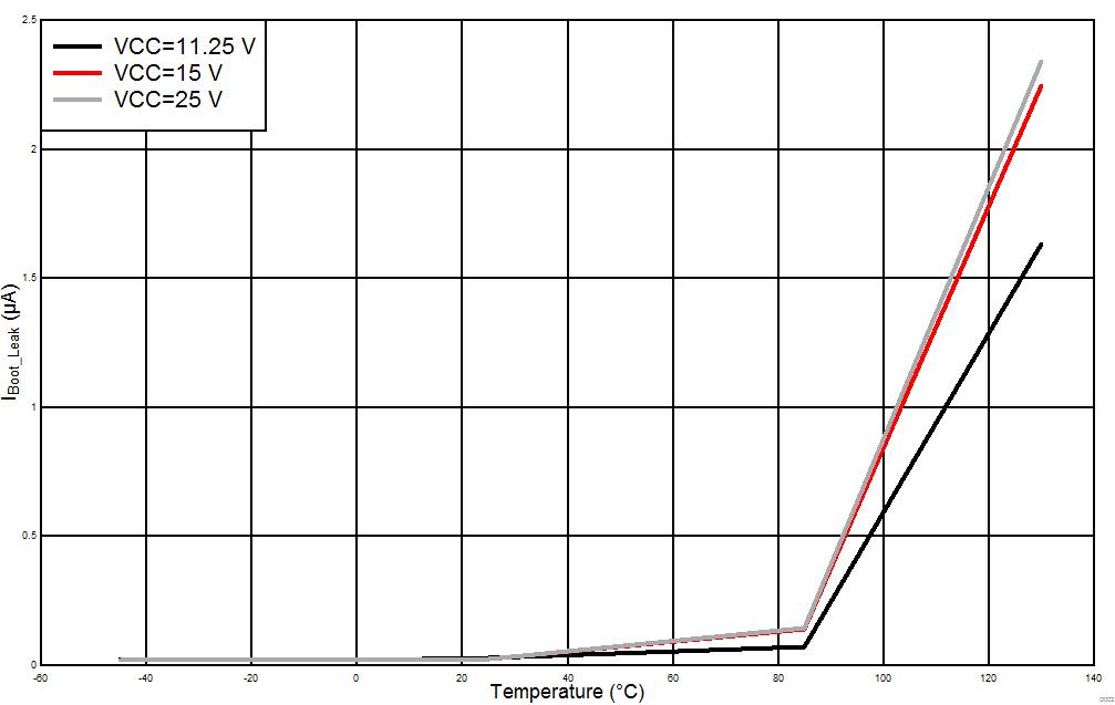
Figure 2. IBOOT_LEAK vs Temperature
UCC256303 D004_SLUSD49.gif
Figure 4. IMISMATCH vs Temperature
UCC256303 D006_SLUSD49.gif
Figure 6. VRVCC vs Temperature, ICC = 100 mA
UCC256303 D008_SLUSD49.gif
Figure 8. iCCSleep vs Temperature
UCC256303 D010_SLUSD49.gif
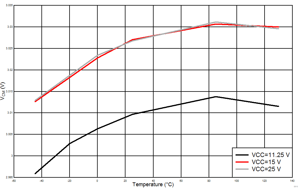
Figure 10. VCM vs Temperature
UCC256303 D012_SLUSD49.gif
Figure 12. IFB vs Temperature
UCC256303 D014_SLUSD49.gif
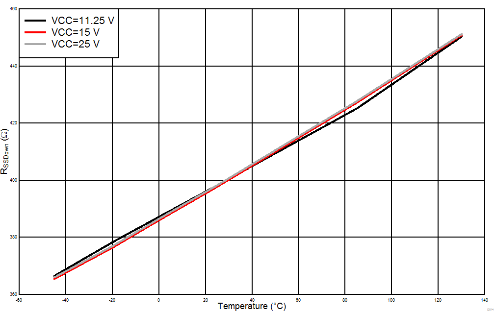
Figure 14. RSSDown vs Temperature
UCC256303 D016_SLUSD49.gif
Figure 16. IHB-HSUVLOFall vs Temperature
UCC256303 D018_SLUSD49.gif
Figure 18. VRVCC-VLOH vs Temperature
UCC256303 D020_SLUSD49.gif
Figure 20. VHB - VHOH vs Temperature